Oscillator
- Summary
- Abstract
- Description
- Claims
- Application Information
AI Technical Summary
Benefits of technology
Problems solved by technology
Method used
Image
Examples
first embodiment
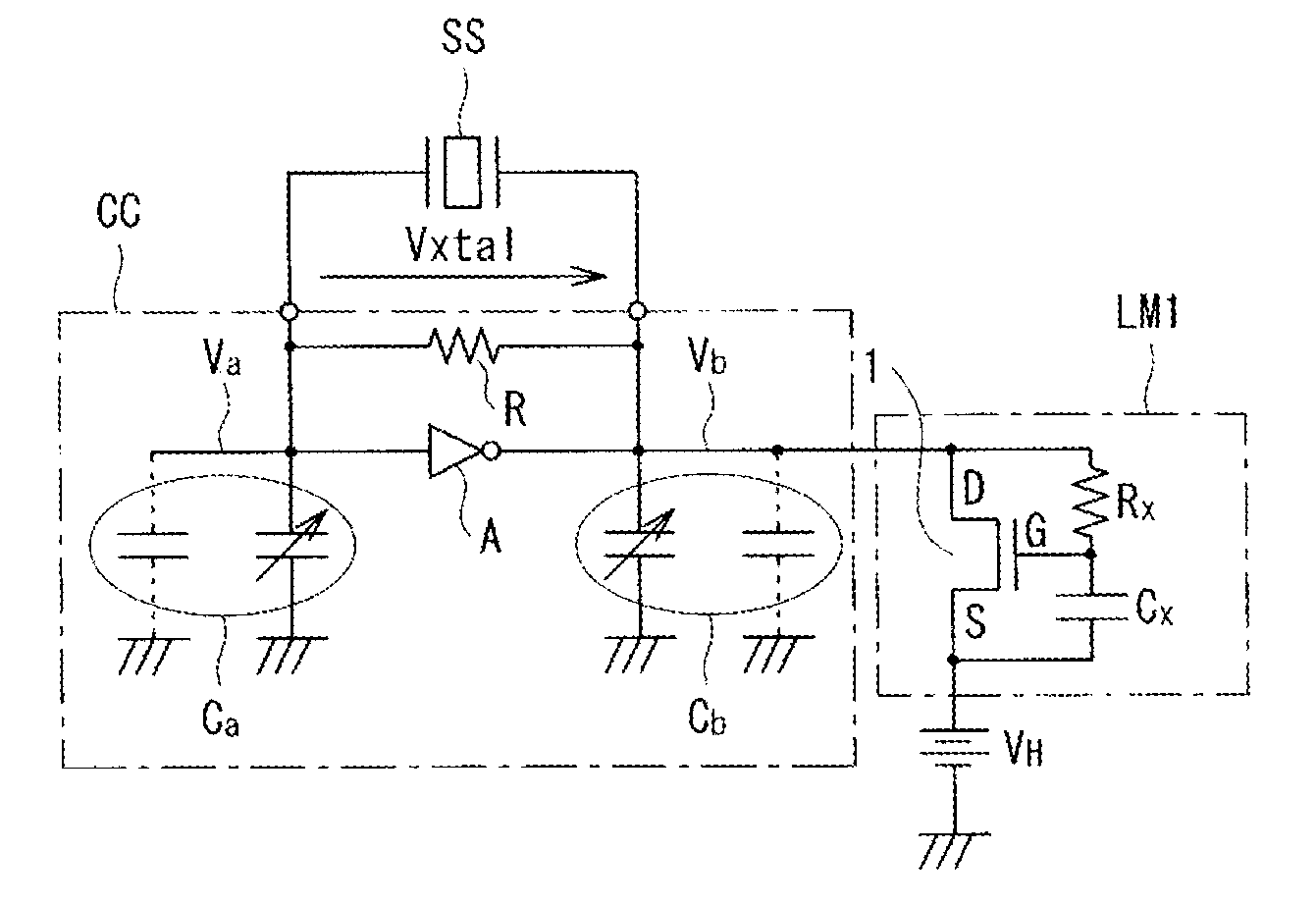
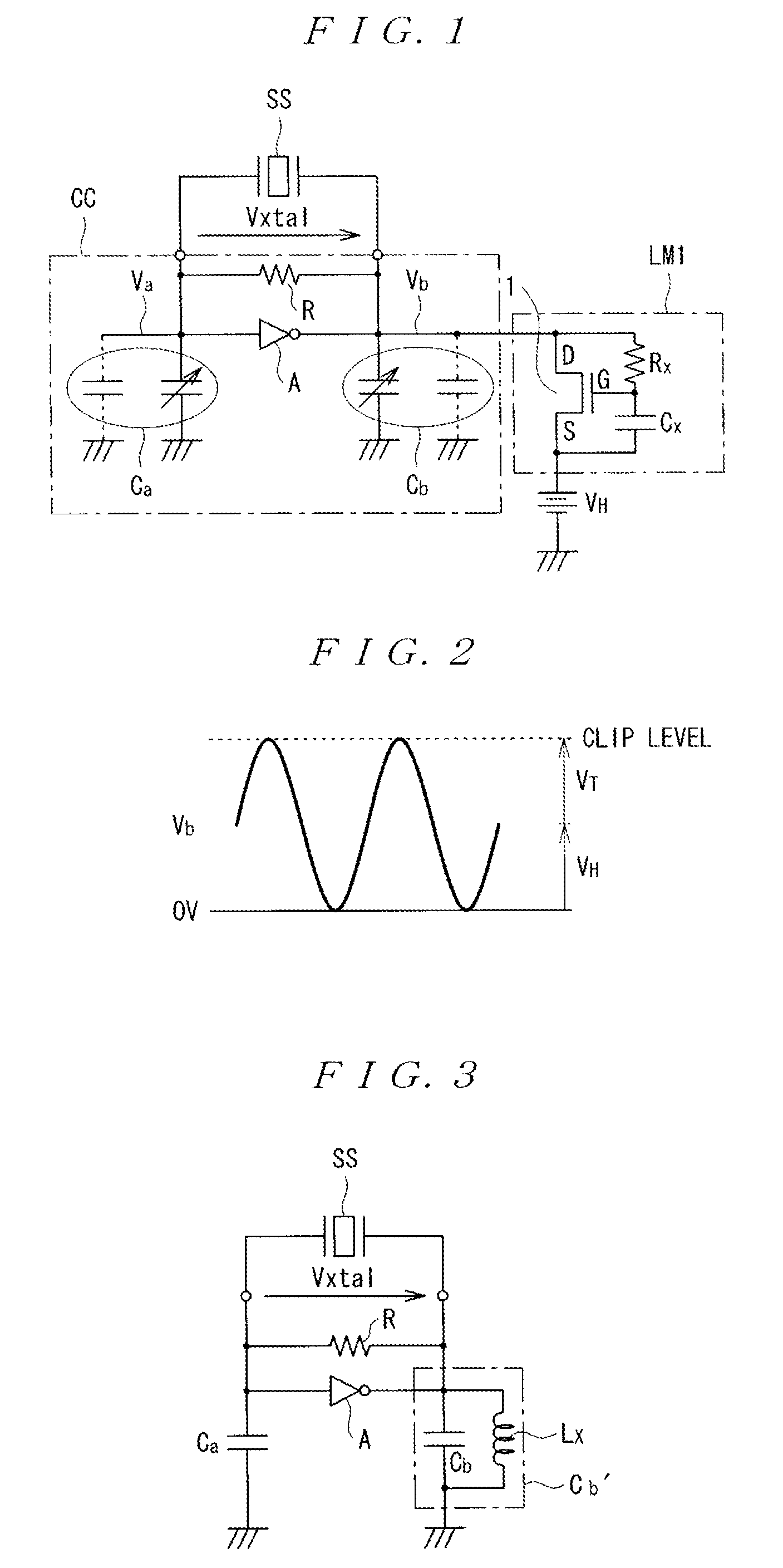
[0060]FIG. 1 is a circuit diagram showing the configuration of an oscillator according to an embodiment of the present invention. In FIG. 1, the oscillator according to this embodiment is configured such that a limiter circuit LM1 is connected as a load circuit of the oscillator which comprises a crystal resonator SS and an oscillation circuit section CC for oscillating the crystal resonator SS.
[0061]The following description will be given in the context of a crystal resonator. However, the resonator to be used is not limited to a crystal resonator. A SAW resonator, a ceramic resonator, or the like may be used instead.
[0062]Focus attention on the limiter circuit LM1 in FIG. 1. Electric current caused by oscillation from one terminal of the crystal resonator passes through the limiter circuit LM1 and returns to the other terminal of the crystal resonator via a voltage source (with a voltage value VH). The limiter circuit LM1 is thus a load of the crystal resonator.
[0063]The limiter c...
second embodiment
[0080]FIG. 7 is a circuit diagram showing the configuration of an oscillator according to a second embodiment of the present invention. The first embodiment described above has a configuration in which a limiter circuit for an upward direction (i.e., a circuit which regulates the upper limit for a varying voltage at the output terminal of the amplifier A when connected to the output terminal is added. In contrast, this embodiment adopts a configuration in which a limiter circuit for a downward direction (i.e., a circuit which regulates the lower limit for a varying voltage at an output terminal of an amplifier A when connected to the output terminal) is further added.
[0081]In FIG. 7, a limiter circuit LM1 for the upward direction and a limiter circuit LM2 for the downward direction are connected as loads of the oscillator. The limiter circuit LM2 in this example comprises an N-type MOS transistor 2, a capacitive element Cx2 which is connected between a gate terminal G and a source t...
third embodiment
[0095]A limiter circuit can also be arranged between terminals of a crystal resonator. For example, a differential limiter circuit L3 may be connected as a limiter circuit for an upward direction between terminals of a crystal resonator SS, as shown in FIG. 10. Note that the potential at a drain terminal of an N-type MOS transistor 1 needs to be DC-biased to be higher than that at a source terminal by a current source Is. For the relationship between a voltage Va and a voltage Vb during oscillation, the action of the voltage Vb starting dropping when the voltage Va starts rising and the action of the voltage Vb starting rising when the voltage Va starts dropping are alternately performed. Assume that a value of the voltage Vb—the voltage Va exceeds a threshold voltage value VT for the N-type MOS transistor when the voltage Va starts dropping, and the voltage Vb starts rising. In this case, electric current flows through the transistor, and a value of the voltage Va—the voltage Vb is...
PUM
 Abstract
Description
Claims
Application Information


