ESD protection device structure

a protection device and electrostatic discharge technology, applied in the direction of emergency protective circuit arrangement, transistor, etc., can solve the problems of gate oxide layer breakdown voltage becoming smaller, gate oxide layer easily burnout, etc., to reduce the trigger voltage and increase the esd pulse

Active Publication Date: 2011-02-24
UNITED MICROELECTRONICS CORP
View PDF14 Cites 10 Cited by
  • Summary
  • Abstract
  • Description
  • Claims
  • Application Information

AI Technical Summary

Benefits of technology

[0009]The present invention implants the second doped region having different conductive type from the first doped region into the first heavy doped region and the first drift region of th

Problems solved by technology

The ESD phenomenon occurs when excess charges are transmitted from the input/output (I/O) pin to the integrated circuit too quickly, which damages the internal circuit.
However, the turned-on voltages of the parasitic bipolar transistors are high, and the gate oxide layer of the NMOS transistor or the PMOS transistor is becoming thinner with the continuing scaling-down of semiconductor integrated circuit (IC) device dimensio

Method used


Image

  • ESD protection device structure
  • ESD protection device structure
  • ESD protection device structure

Examples


first embodiment

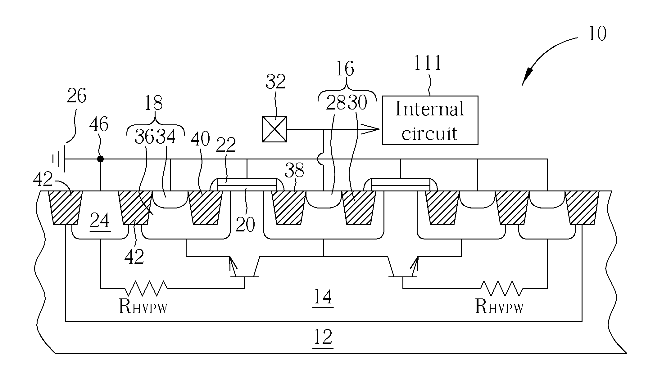
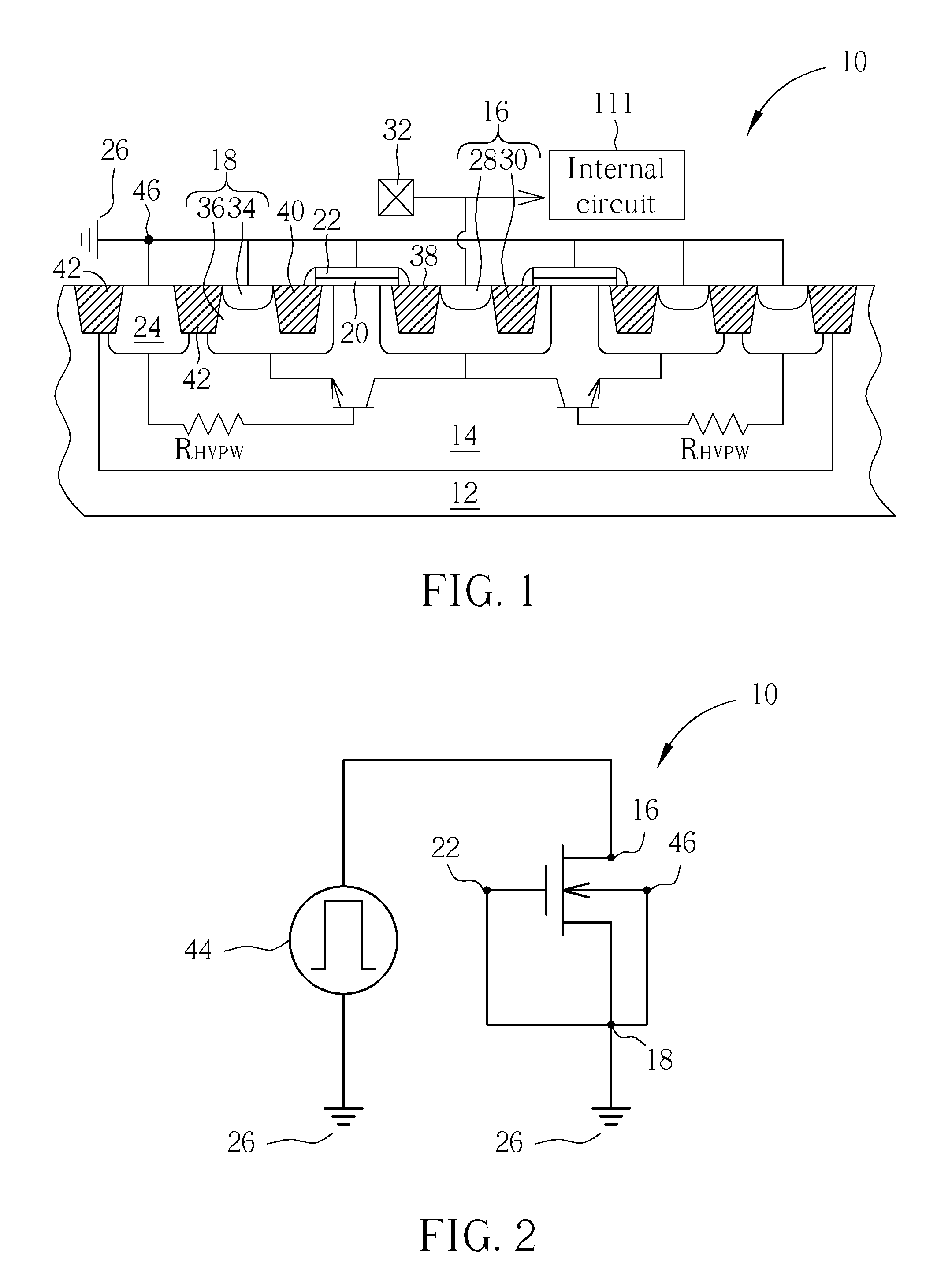
[0022]Please refer to FIG. 1, which is a cross-sectional schematic diagram illustrating an electrostatic discharge (ESD) protection device structure according to the present invention. As shown in FIG. 1, the ESD protection device structure 10 is disposed in a semiconductor substrate 12, and the ESD protection device structure 10 includes a well 14, a drain region 16, a source region 18, a gate dielectric layer 20, a gate electrode 22, and a doped region 24. The well 14 has a first conductive type, such as N-type or P-type, and is disposed in the semiconductor substrate 12. The drain region 16 and the source region 18 are respectively disposed in the well 14. The drain region 16 has a second conductive type, and the source region 18 also has the second conductive type.

[0023]The first embodiment takes the first conductive type being P-type and the second conductive type being N-type as an example. On the contrary, when the first conductive type is N-type, the second conductive type i...

second embodiment

[0027]Please refer to FIG. 5, which is a cross-sectional schematic diagram illustrating an ESD protection device structure according to the present invention. As shown in FIG. 5, the ESD protection device structure 100 is disposed in a semiconductor substrate 102, and the ESD protection device structure 100 includes a well 104 having a first conductive type, a first doped region 106 having a second conductive type and used to be a drain, a second doped region 108 having the first conductive type, and a third doped region 110 having the second conductive type and used to be a source. Similarly, when the first conductive type is P-type, the second conductive type is N-type. On the contrary, when the first conductive type is N-type, the second conductive type is P-type.

[0028]The second embodiment takes the first conductive type being P-type as an example, and the well 104 is a high voltage P-well (HVPW) disposed in the semiconductor substrate 102. The N-type first doped region 106 is d...


PUM


Abstract

An ESD protection device structure includes a well having a first conductive type, a first doped region having a second conductive type disposed in the well, a second doped region having the first conductive type, and a third doped region having the second conductive type disposed in the well. The second doped region is disposed within the first doped region so as to form a vertical BJT, and the first doped region, the well and the third doped region forms a lateral BJT, so that pulse voltage that the ESD protection structure can tolerate can be raised.

Description

BACKGROUND OF THE INVENTION[0001]1. Field of the Invention[0002]The present invention relates to an electrostatic discharge (ESD) protection device structure, and more particularly, to an ESD protection device structure of a gate-grounded metal-oxide-semiconductor transistor.[0003]2. Description of the Prior Art[0004]Electrostatic discharge (ESD) usually occurs in semiconductor devices. The ESD phenomenon occurs when excess charges are transmitted from the input / output (I / O) pin to the integrated circuit too quickly, which damages the internal circuit. In order to solve such a problem, manufacturers normally build an ESD protection device between the internal circuit and the I / O pin. The ESD protection device is initiated before the ESD pulse enters the internal circuit for discharging the excess charges, and thus ESD-related damage is decreased.[0005]Recently, in order to prevent the internal circuit from damage generated by ESD phenomenon, the prior-art ESD protection device uses ...

Claims


Application Information

Patent Timeline
IPC IPC(8): H01L29/73H01L27/102
CPCH01L27/0266
Inventor LAI, TAI-HSIANGFAN, KUEI-CHIHTANG, TIEN-HAO
Owner UNITED MICROELECTRONICS CORP
Why Eureka
Try Eureka