Liquid crystal display device

a liquid crystal display and display device technology, applied in non-linear optics, instruments, optics, etc., can solve the problems of reducing yield, difficult to achieve a high luminance, and sometimes disconnected lines to supply signals, so as to minimize the decrease in optical transmittance and repair defects more easily

Inactive Publication Date: 2011-02-24
SHARP KK
View PDF10 Cites 14 Cited by
  • Summary
  • Abstract
  • Description
  • Claims
  • Application Information

AI Technical Summary

Benefits of technology

[0044]The present invention provides a liquid crystal display device that can not only repair defects more easily but also minimize the decrease in optical transmittance.

Problems solved by technology

In an actual active-matrix substrate, however, lines to supply signals may sometimes be disconnected or leakage current may flow between two conductive members that should be electrically insulated from each other.
An LCD that has been fabricated using such an active-matrix substrate could not be supplied with a normal voltage and might produce a point defect, a line defect and other defects, thus resulting in a lower yield eventually.
On top of that, in the MVA-mode LCD, a region with a slit or a rib has a decreased transmittance, and it is difficult to achieve a high luminance.
They say that those domain lines are produced because the reference alignment directions of the liquid crystal domains and the directions of the alignment control forces produced by an oblique electric field generated at the edges of the pixel electrode have mutually opposing components, thus disturbing the alignment of the liquid crystal molecules there.

Method used


Image

  • Liquid crystal display device
  • Liquid crystal display device
  • Liquid crystal display device

Examples


embodiment 1

[0087]Hereinafter, a First Embodiment of a Liquid Crystal display device according to the present invention will be described.

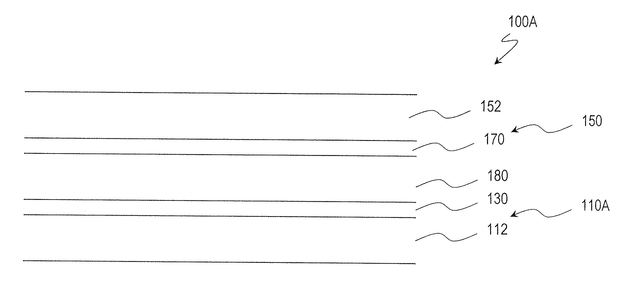
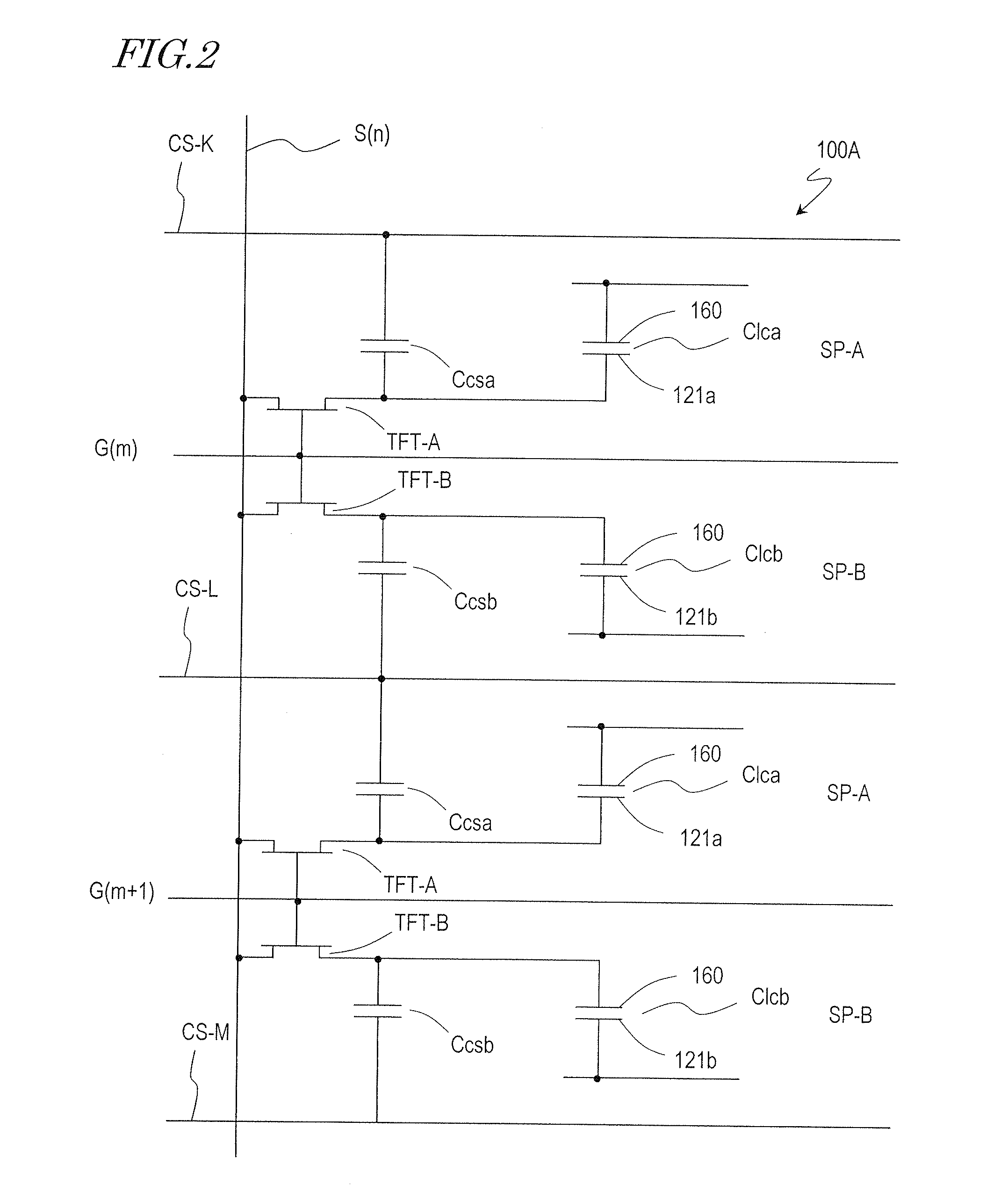
[0088]FIG. 1 is a schematic representation illustrating a liquid crystal display device 100A in this embodiment. The liquid crystal display device 100A includes an active-matrix substrate 110A, a counter substrate 150 and a liquid crystal layer 180. The active-matrix substrate 110A includes a first alignment film 130 that is supported on an insulating substrate 112. On the other hand, the counter substrate 150 includes a second alignment film 170 supported on a transparent insulating substrate 152. A liquid crystal layer 180 is arranged between the first and second alignment films 130 and 170 of the active-matrix substrate 110A and the counter substrate 150. Although not shown in FIG. 1, multiple lines and pixel electrodes are arranged between the insulating substrate 112 of the active-matrix substrate 110A and the first alignment film 130. And a counter elec...

embodiment 2

[0171]Hereinafter, a second embodiment of a liquid crystal display device according to the present invention will be described.

[0172]FIG. 13(a) is a schematic plan view illustrating the configuration of an active-matrix substrate 110B for the liquid crystal display device 100B of the second embodiment. FIG. 13(b) is a schematic plan view illustrating how dark lines are produced in the liquid crystal display device 100B of this embodiment. And FIG. 13(c) is a schematic plan view illustrating the liquid crystal display device 100B.

[0173]The liquid crystal display device 100B of this embodiment has substantially the same structure as the liquid crystal display device 100A described above, and the overlapping description thereof will be omitted herein. The liquid crystal display device 100B is different from this liquid crystal display device 100A in that the dark lines are produced in an inverted swastika shape.

[0174]In FIG. 13(a), illustrated are the second subpixel SP-B of a pixel on...

embodiment 3

[0206]Hereinafter, a third embodiment of a liquid crystal display device according to the present invention will be described.

[0207]FIG. 22(a) is a schematic plan view illustrating the configuration of the active-matrix substrate 110C of a liquid crystal display device 100C as a third embodiment of the present invention. FIG. 22(b) is a schematic plan view illustrating how dark lines are produced in the liquid crystal display device 100C of this embodiment. And FIGS. 22(c) and 22(d) are schematic plan views of the liquid crystal display device 100C. Specifically, FIG. 22(c) indicates where dark lines are produced and where ribs or slits (openings) are arranged in the liquid crystal display device 100C, while FIG. 22(d) illustrates the pattern of the black matrix BM.

[0208]The liquid crystal display device 100C of this embodiment has a similar structure to the liquid crystal display devices 100A and 100B described above, and the overlapping description thereof will be omitted herein. ...


PUM

PropertyMeasurementUnit
angleaaaaaaaaaa
pretilt angleaaaaaaaaaa

Abstract

In the liquid crystal display device (100A) of the present invention, the pixel electrode (121) has a notch (122a2) provided for a portion of a line. If the azimuthal component of liquid crystal molecules (182), located approximately at the middle of the thickness of a liquid crystal layer (180) in an area where the respective alignment regions of first and second alignment films (130) and (170) overlap with each other to a viewer's eye, is called a “reference alignment azimuth”, an oblique electric field, generated by a counter electrode (160) and the notch (122a2) of the pixel electrode (121) upon the application of a voltage, causes the azimuthal component of the liquid crystal molecules (182) in a region of the liquid crystal layer (180) associated with at least a portion of the notch (122a2) of the pixel electrode (121), to intersect with the reference alignment azimuth at an angle of 90 degrees or less.

Description

TECHNICAL FIELD[0001]The present invention relates to a liquid crystal display device.BACKGROUND ART[0002]A liquid crystal display (LCD) is a display device with significantly reduced thickness and power dissipation, and has found a broad variety of applications in various fields. Among other things, an active-matrix-addressed LCD, including a switching element such as a thin-film transistor (TFT) for each pixel, has such high contrast ratio, excellent response characteristic and high performance as to be applied to TVs, monitors, laptops, and so on. And the LCD market has been expanding faster and faster year after year.[0003]An active-matrix-addressed LCD includes an active-matrix substrate, on which a number of switching elements are arranged, and a counter substrate, which faces the active-matrix substrate, and conducts a display operation by controlling the optical transmittance of a liquid crystal layer interposed between those two substrates. The active-matrix substrate is fa...

Claims


Application Information

Patent Timeline
Patent Type & Authority Applications(United States)
IPC IPC(8): G02F1/1343
CPCG02F1/133707G02F2001/134345G02F1/133753G02F1/134345
Inventor HIRATO, SHINICHI
Owner SHARP KK
Why Eureka
Try Eureka