Electrochromic devices, assemblies incorporating electrochromic devices, and/or methods of making the same

a technology of electrochromic devices and electrochromic devices, which is applied in the direction of door/window protective devices, non-linear optics, instruments, etc., can solve the problems of excessive heating costs, significant waste of energy, and excessive cooling, and achieve greater solar heat gain control (shgc) delta, improved appearance, and visible transmission

Active Publication Date: 2011-03-03
GUARDIAN GLASS LLC
View PDF34 Cites 105 Cited by
  • Summary
  • Abstract
  • Description
  • Claims
  • Application Information

AI Technical Summary

Benefits of technology

[0017]One aspect of certain example embodiments involves the incorporation of novel electrochromic materials. For example, certain example embodiments involve an optically doped cathode and/or anode for greater visible transmission in the clear state, greater solar heat gain control (SHGC) delta between these states, improved appearance, and better reliability. Controlling the stoichiometry of WOx (e.g., so that it is sub-stoichiometric) advantageously may result in improvements with respect to the SHGC delta and better appearance (e.g., in terms of coloration). Anodically coloring the counter electrode also may increase the SHGC delta.
[0018]Another aspect of certain example embodiments involves the incorporation of a novel electrochromic device stack. For example, the inclusion of a low-cost, low-Fe mid-lite substrate may help reduce the need for substrate-device barrier layers. An improved transparent current collector (TCC) with much higher conductivity and transmittance than ITO may be provided for increased switching speed and reduced cost. The inclusion of a lithium phosphorus oxynitride (LiPON) electrolyte material may be selected for reliability purposes in certain example embodiments. Additionally, the use of transparent dielectric/conductive layers may be used to shift the col...

Problems solved by technology

However, they also represent a significant source of wasted energy.
Current window technology often leads to excessive heating costs in winter, excessive cooling in summer, and often fails to capture the benefits of daylight, that would allow lights to be dimmed or turned off in much of the nation's commercial stock.
Another drawback with current lithium-based inorganic ECWs relates to their slow switching times. Indeed, current switching times for lithium-based inorganic ECWs typically range from about 5-10 minutes.
Proton-based inorganic and organic polymer device mechanisms switch somewhat faster (e.g., 15 seconds to 5 minutes) but unfortunately suffer from degradation of the ionic conductor in the former case and degradation of the polymer in the latter case.
Unfortunately, current ECW films do not meet the required performance in appearance (including color), switching speed, quality consistency, and long term reliability.
Adequate supply and useful window sizes are additional issues.
One reason the current high ECW cost structure is above the market threshold is that the EC device fabrication is incompatible the fabricat...

Method used


Image

  • Electrochromic devices, assemblies incorporating electrochromic devices, and/or methods of making the same
  • Electrochromic devices, assemblies incorporating electrochromic devices, and/or methods of making the same
  • Electrochromic devices, assemblies incorporating electrochromic devices, and/or methods of making the same

Examples


example fabrication

Processes

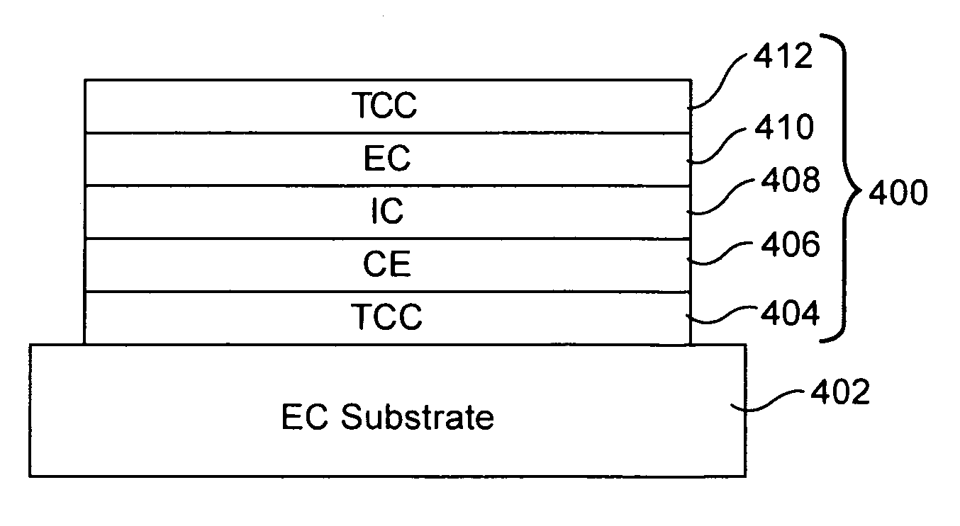
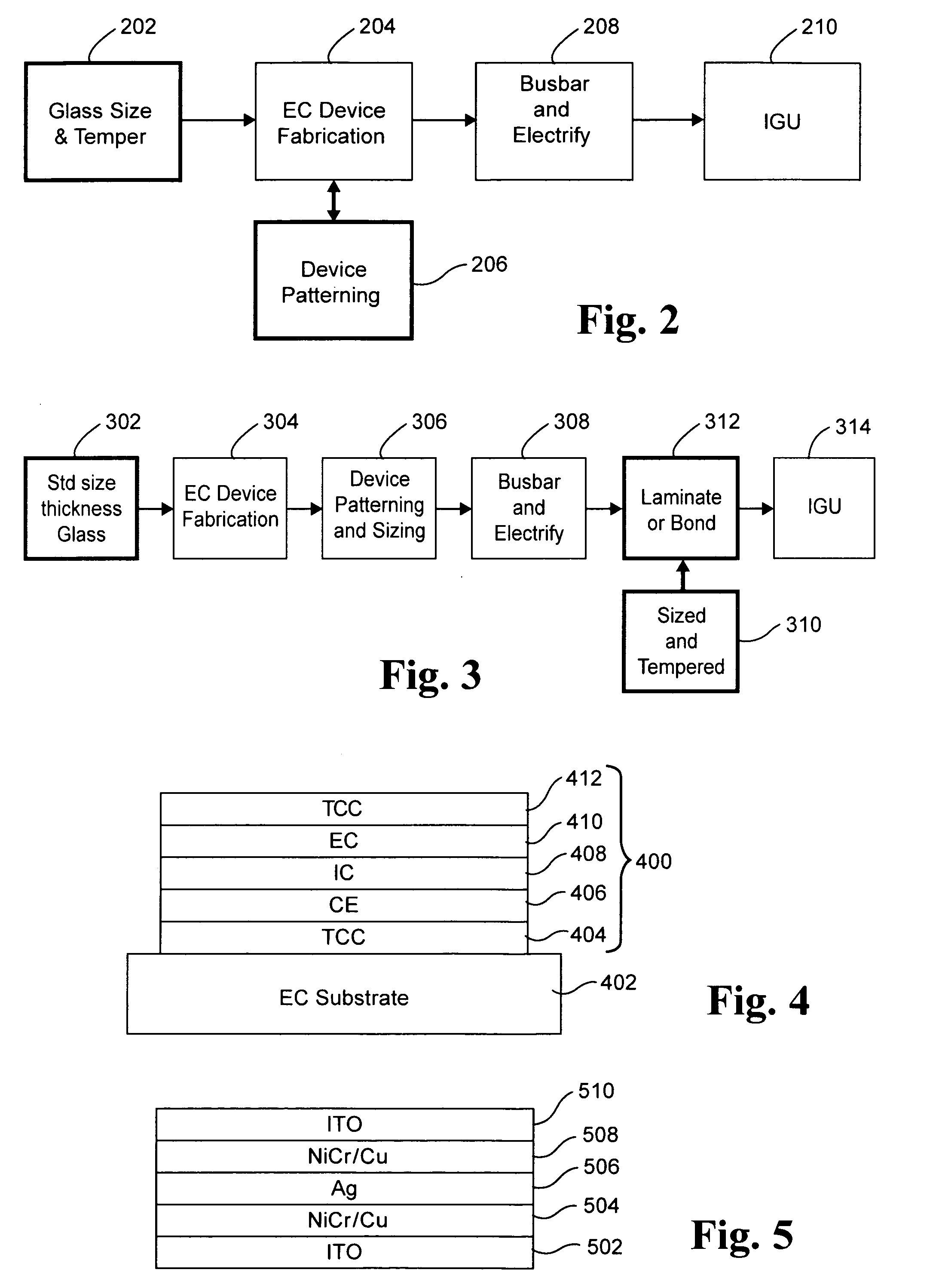
[0046]FIG. 3 is a block diagram illustrating an ECW fabrication process in accordance with an example embodiment. The FIG. 3 process differs from the FIG. 2 process in several ways, owing to the fact that the FIG. 3 process is designed to provide an EC device on an EC substrate that may be bonded, laminated, or otherwise connected to a temperable substrate. For example, a material such as PVB, EVA, or the like may be used, as may “optibond technology,” which is commercially available from Litemax. The laminate that is used may incorporate a UV blocker (e.g., a UVA blocker). Preferably, a UVA blocker may be included, with Tuv<1%, more preferably <0.75%, and still more preferably <0.5%. The UV blocker may a thin film coating comprising one or more of Bi, BiO, Zn, ZnO, TiO, BiSnO, AgO, Ce, CeO, and / or the like. Alternatively, or in addition, a PET coating may be provided, with a UV blocking material provided thereon and / or therein. For example, an ITO-coated PET layer may be p...

example process

Integration Techniques

[0072]One drawback associated with traditional EC process flows is the need for substrate sizing and tempering before EC device formation, which is related to the fact that post-fabrication tempering will damage the EC device and sizing cannot be performed after tempering. This conventional process flow was illustrated in FIG. 2. In this process, any variation in finished product requirement such as, for example, substrate size, thickness or type, etc., tends to lead to a complex device / layer manufacturing environment. For example, the EC coating process will be fine-tuned to each product separately for optimum results depending on, for example, the substrate size and thickness. For applications such as ECW, with distinct contrast, especially at tinted state, such non-uniformity would be detrimental to the product.

[0073]However, as indicated above (e.g., in connection with FIG. 3), certain example embodiments instead involve lamination, a non-tempered single ty...


PUM

PropertyMeasurementUnit
Sheet resistanceaaaaaaaaaa
Volumeaaaaaaaaaa
Volumeaaaaaaaaaa

Abstract

Certain example embodiments of this invention relate to electrochromic (EC) devices, assemblies incorporating electrochromic devices, and/or methods of making the same. More particularly, certain example embodiments of this invention relate to improved EC materials, EC device stacks, high-volume manufacturing (HVM) compatible process integration schemes, and/or high-throughput low cost deposition sources, equipment, and factories.

Description

CROSS-REFERENCE TO RELATED APPLICATION[0001]This application claims the benefit of U.S. Application Ser. No. 61 / 237,580, filed on Aug. 27, 2009, the entire contents of which are hereby incorporated herein by reference.FIELD OF THE INVENTION[0002]Certain example embodiments of this invention relate to electrochromic (EC) devices, assemblies incorporating electrochromic devices, and / or methods of making the same. More particularly, certain example embodiments of this invention relate to improved EC materials, EC device stacks, high-volume manufacturing (HVM) compatible process integration schemes, and / or high-throughput low cost deposition sources, equipment, and factories.BACKGROUND AND SUMMARY OF EXAMPLE EMBODIMENTS OF THE INVENTION[0003]Windows provide natural light, fresh air, access, and connection to the outside world. However, they also represent a significant source of wasted energy. With the growing trend in increasing the use of architectural windows, balancing the conflicti...

Claims


Application Information

Patent Timeline
IPC IPC(8): B32B38/00B32B37/14G02F1/1524
CPCB32B17/10045Y10T156/10B32B17/10174B32B17/10761B32B17/10981E06B3/6722E06B9/24E06B2009/2464G02F1/1508G02F1/1523G02F1/1525G02F1/1533G02F1/15Y10T156/1062B32B17/10055G02F1/1524
Inventor VEERASAMY, VIJAYEN S.
Owner GUARDIAN GLASS LLC
Why Eureka
Try Eureka