Touch panel and a method of locating a touch point of the same

a technology of touch panel and touch point, which is applied in the field of touch panel, can solve the problems of inability to improve the yield ratio of the touch panel, inability to reduce the cost and time of production, and inability to further upgrade the touch control precision of the conventional touch panel

Active Publication Date: 2011-03-03
INNOLUX CORP
View PDF2 Cites 13 Cited by
  • Summary
  • Abstract
  • Description
  • Claims
  • Application Information

AI Technical Summary

Benefits of technology

A conventional capacitive-type touch panel includes two pattern layers made of transparent conductive materials formed on two surfaces of a glass substrate respectively to detect two-dimensional coordinates on the pattern layers. The transparent conductive material of conventional touch panel is indium tin oxide (ITO, and the manufacture of the touch panel uses semiconductor manufacture technologies such as photolithography, exposure and etching technologies etc. Due to the multiplicity or complexity of the process steps, the yield ratio of the touch panel can not be improved, and the cost and time of production can not be decreased either. Moreover, due to the limitation of the process resolution, touch control precision of the conventional touch panels can not be further upgraded.

Problems solved by technology

Due to the multiplicity or complexity of the process steps, the yield ratio of the touch panel can not be improved, and the cost and time of production can not be decreased either.
Moreover, due to the limitation of the process resolution, touch control precision of the conventional touch panels can not be further upgraded.

Method used


Image

  • Touch panel and a method of locating a touch point of the same
  • Touch panel and a method of locating a touch point of the same
  • Touch panel and a method of locating a touch point of the same

Examples


first embodiment

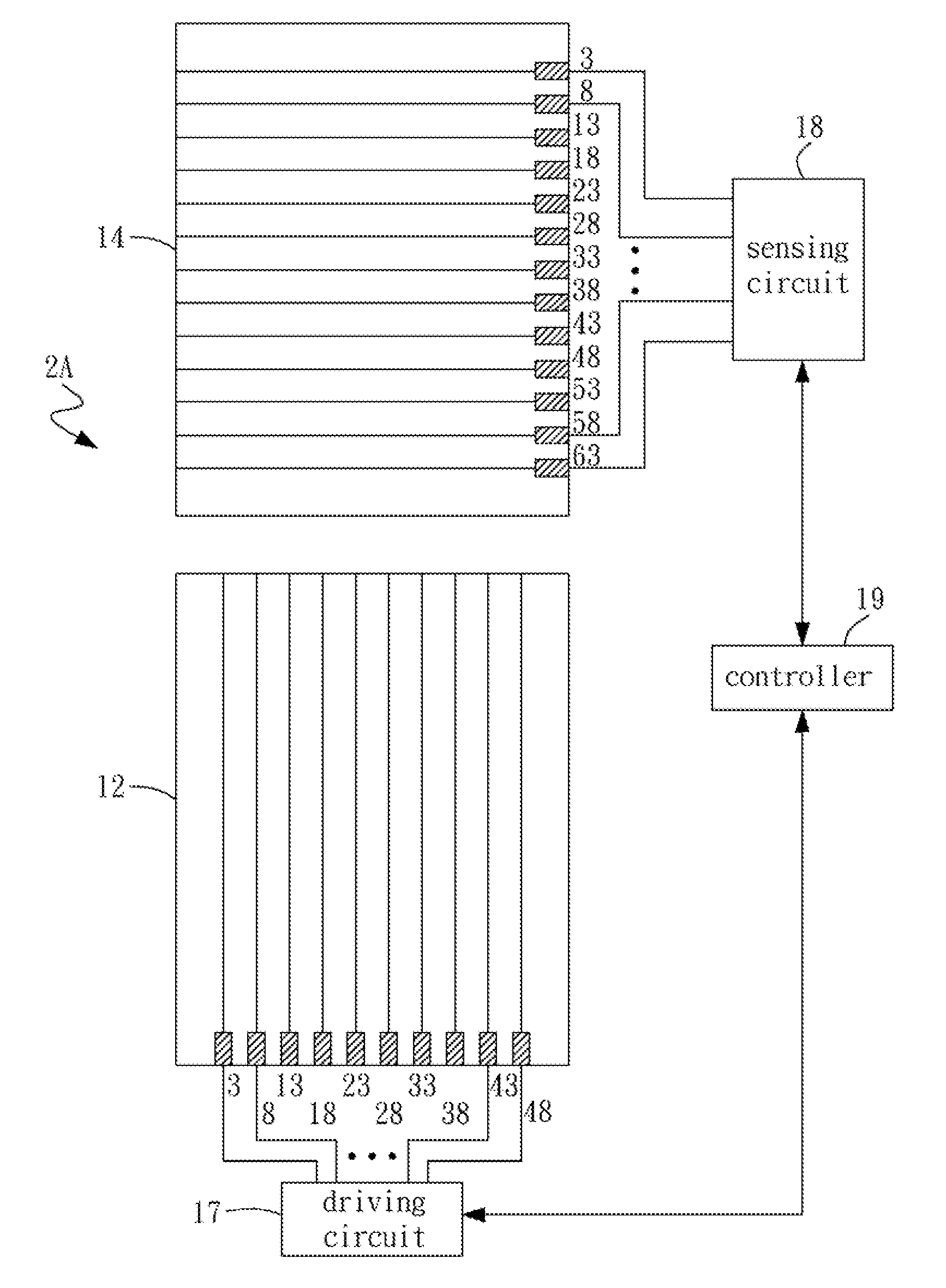
FIG. 2A shows a touch point locating system 2A of the touch panel of the present disclosure. The impedance of the first conductive film 12 along the second direction such as y-axis or a longitudinal axis is minimum and relatively less than the impedance along other directions. The impedance of the second conductive film 14 along the first direction such as x-axis or a transverse axis is minimum and relatively less than the impedance along other directions. Each first pad 120 connects to an electronic signal input circuit or a driving circuit 17 via conductive lines. The driving circuit 17 inputs electronic signals with the same pulse waveform or other waveforms to each first pad 120 in sequence or simultaneously. Each second pad 140 connects to an electronic signal readout circuit or a sensing circuit 18 via conductive lines to read out sensed electronic signals of each second pad 140. The first pad 120 is used as the driving electronic signal pad, while the second pad 140 is used a...

second embodiment

FIG. 3A shows a touch point locating system 2B of the touch panel of the present disclosure. Similar to the touch point locating system shown in FIG. 2A, the impedance of the first conductive film 12 along the second direction such as y-axis or a longitudinal axis is minimum and relatively less than the impedance along other directions. The impedance of the second conductive film 14 along the first direction such as x-axis or a transverse axis is minimum and relatively less than the impedance along other directions. The differences are in that each second pad 140 connects to an electronic signal input circuit or a driving circuit 17 via conductive lines. The driving circuit 17 inputs electronic signals with the same pulse waveform or other waveforms to each first pad 140 in sequence or simultaneously. Each first pad 120 connects to an electronic signal readout circuit or a sensing circuit 18 via conductive lines to read out sensed electronic signals of each second pad 120. The secon...


PUM


Abstract

The present disclosure is directed to a touch panel and a method of locating a touch point. An insulating layer is disposed between a first insulating substrate and a second insulating substrate. A first conductive film with anisotropic impedance is disposed between the first insulating substrate and the insulating layer, and a second conductive film with anisotropic impedance is disposed between the insulating layer and the second insulating substrate. Multiple first pads are disposed on a peripheral region of the first conductive film along a first direction, and multiple second pads are disposed on a peripheral region of the second conductive film along a second direction. The first conductive film has least impedance along the second direction, and the second conductive film has least impedance along the first direction.

Description

BACKGROUND1. Technical FieldThe present disclosure relates to a touch panel, and more particularly to a touch panel having conductive films with anisotropic impedance and a method of locating a touch point.2. Description of Related ArtTouch panels or touch screens are widely applied in electronic apparatuses, particularly in portable or hand-held electronic apparatuses, such as personal digital assistants (PDA) or mobile phones. Touch panels involve integration of resistive-type, capacitive-type or optical touch technologies and display panels.A conventional capacitive-type touch panel includes two pattern layers made of transparent conductive materials formed on two surfaces of a glass substrate respectively to detect two-dimensional coordinates on the pattern layers. The transparent conductive material of conventional touch panel is indium tin oxide (ITO, and the manufacture of the touch panel uses semiconductor manufacture technologies such as photolithography, exposure and etchi...

Claims


Application Information

Patent Timeline
Patent Type & Authority Applications(United States)
IPC IPC(8): G06F3/045
CPCG06F3/044G06F3/0446G06F3/0445G06F3/04166
Inventor LIAO, TAI-SHUNPAN, HSUAN-LINSHIH, PO-SHENG
Owner INNOLUX CORP
Why Eureka
Try Eureka