

Memory circuit structure and semiconductor process for manufacturing the same
a technology of memory circuit and semiconductor, applied in semiconductor devices, semiconductor/solid-state device details, electrical devices, etc., can solve the problems of significant amplification, difficult to form pattern features with good profile characteristics, and formidable challenges of conventional photolithographic technologies
- Summary
- Abstract
- Description
- Claims
- Application Information
AI Technical Summary
Benefits of technology
Problems solved by technology
Method used
Image

Examples
Embodiment Construction
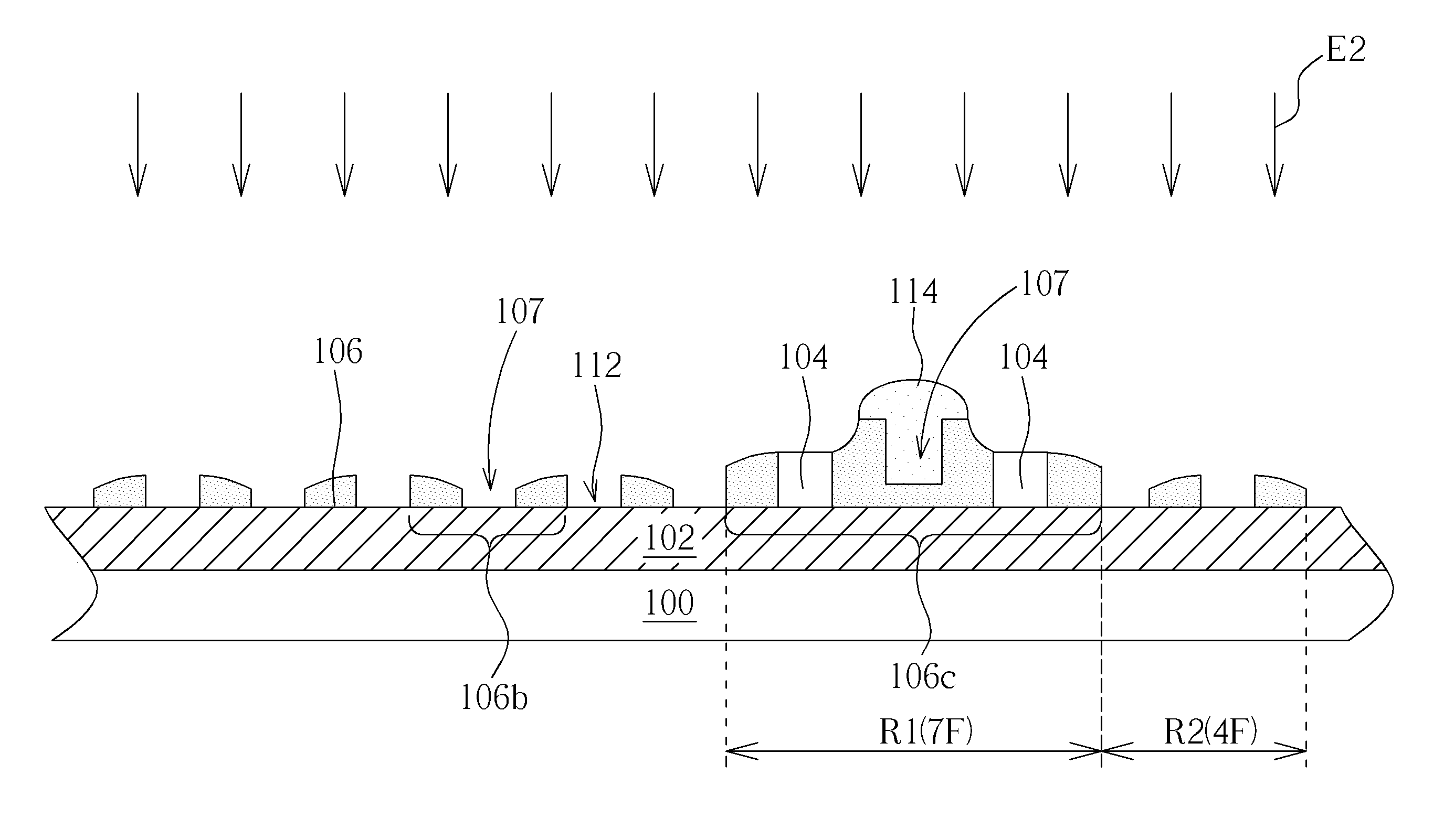
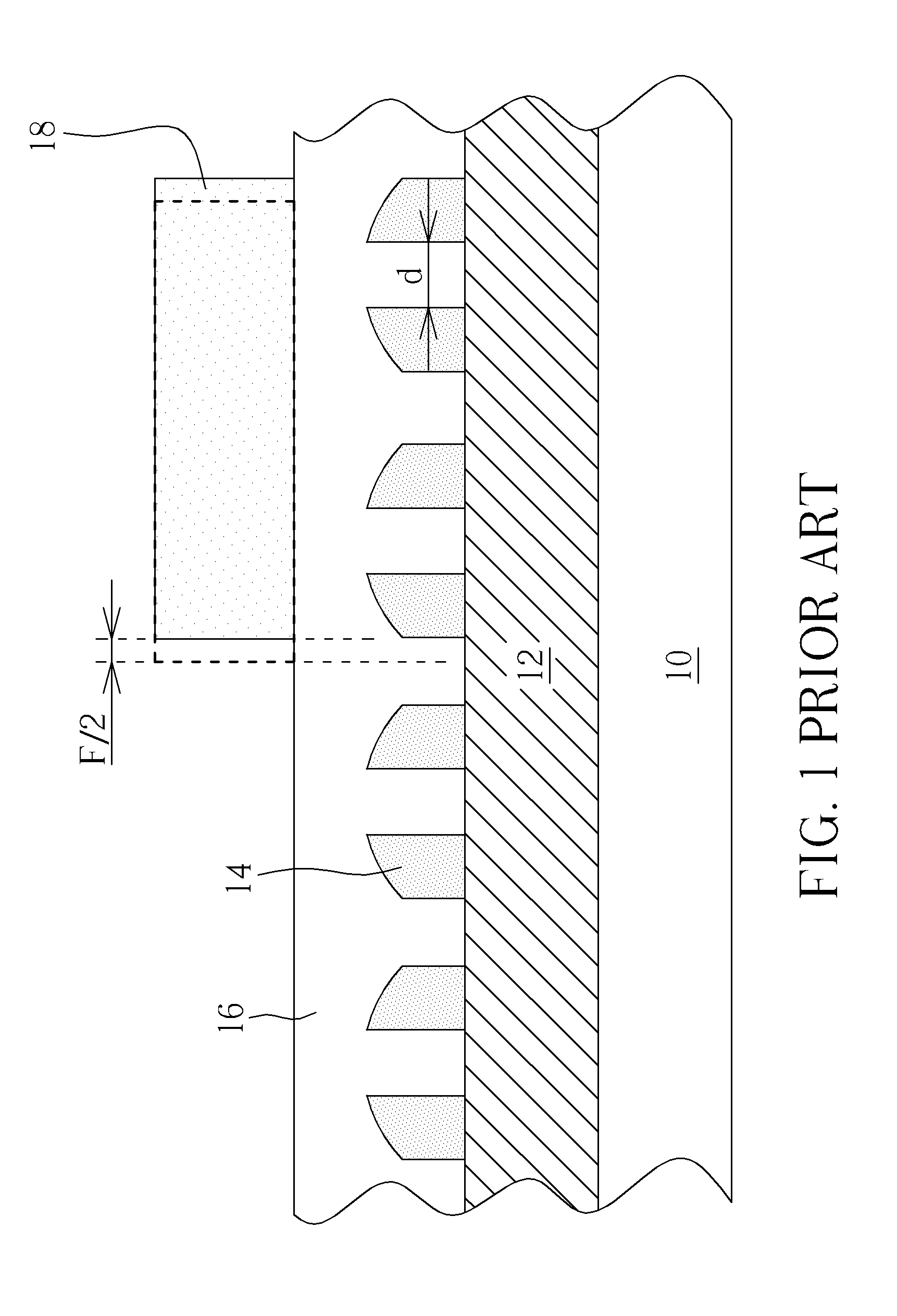
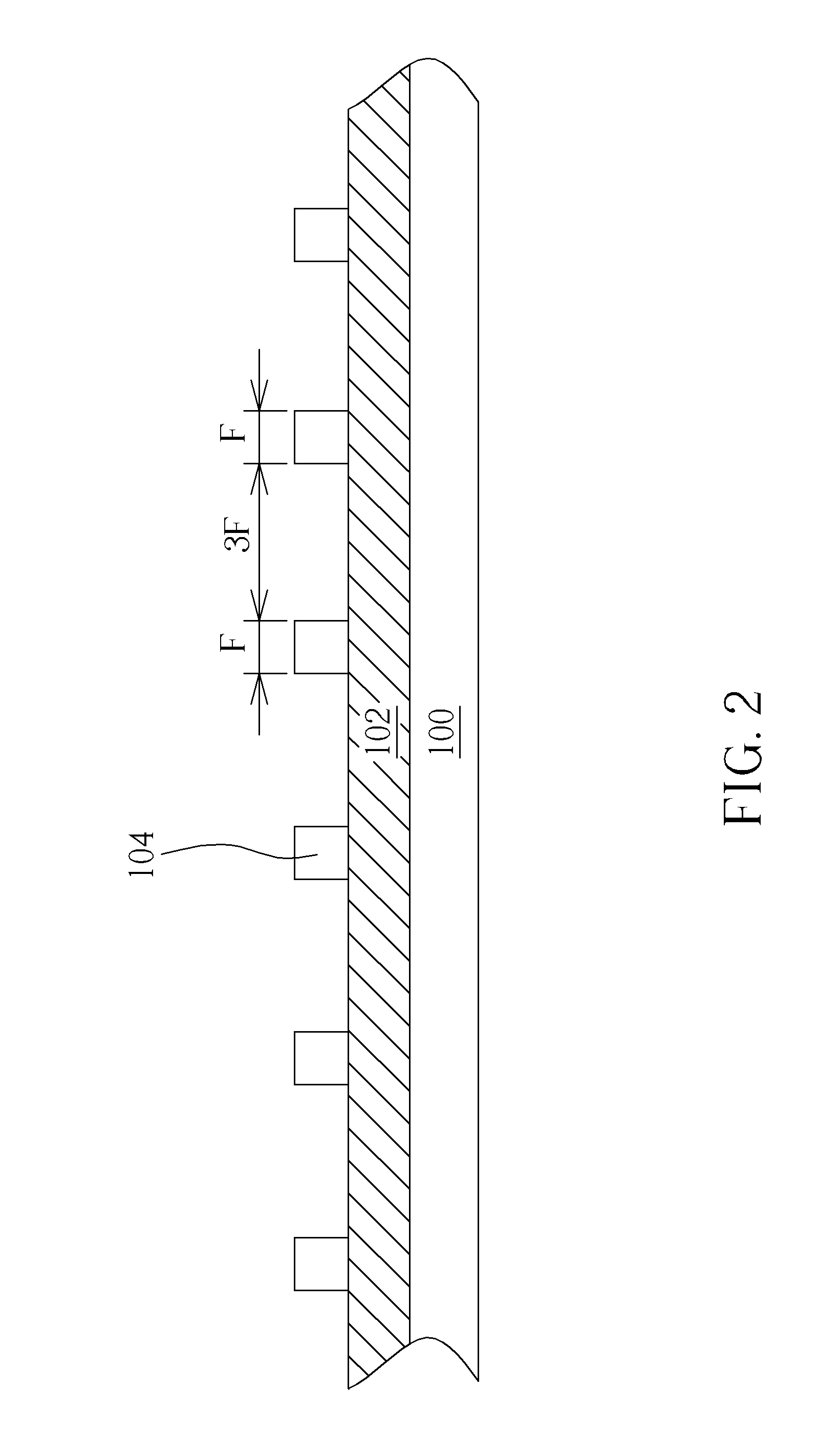
[0018]In the following detailed description, reference is made to the accompanying drawings which form a part hereof and is shown by way of illustration and specific embodiments in which the invention may be practiced. These embodiments are described in sufficient details to enable those skilled in the art to practice the present invention. It should be noted that the present invention may utilize other embodiments, or structural, logical, and electrical changes maybe made without departing from the scope of the present invention. Therefore, the following detailed description is not intended to be taken in a limiting sense, and the scope of the present invention is defined by the appended claims. Furthermore, certain terms are used throughout following description and appended claims to refer to particular components. As one skilled in the art will comprehend, the manufacturers of the semiconductor device may refer to a component as different names, such as spacer, liner, insulators...
PUM
 Abstract
Description
Claims
Application Information