Adhesive film with dicing sheet and method of manufacturing the same
- Summary
- Abstract
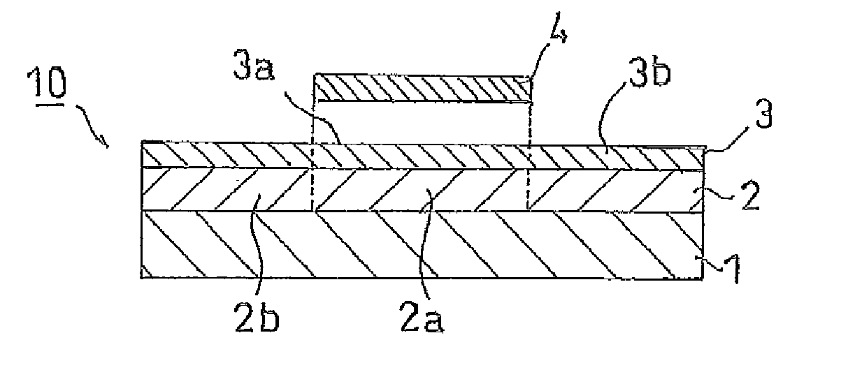
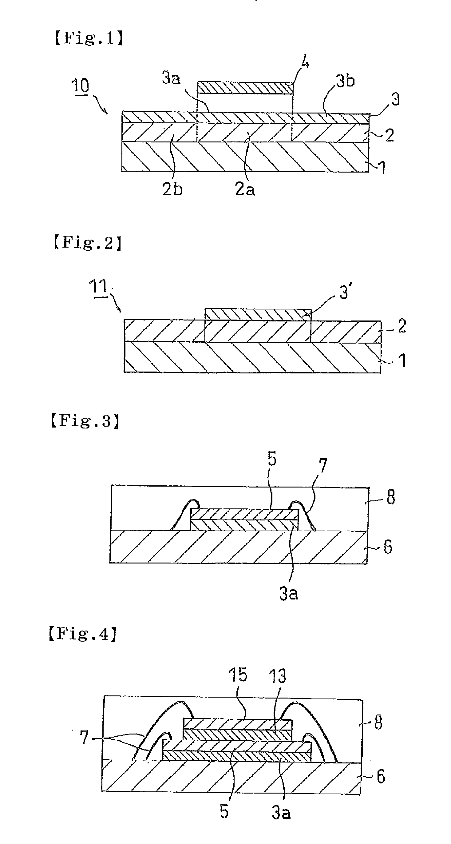
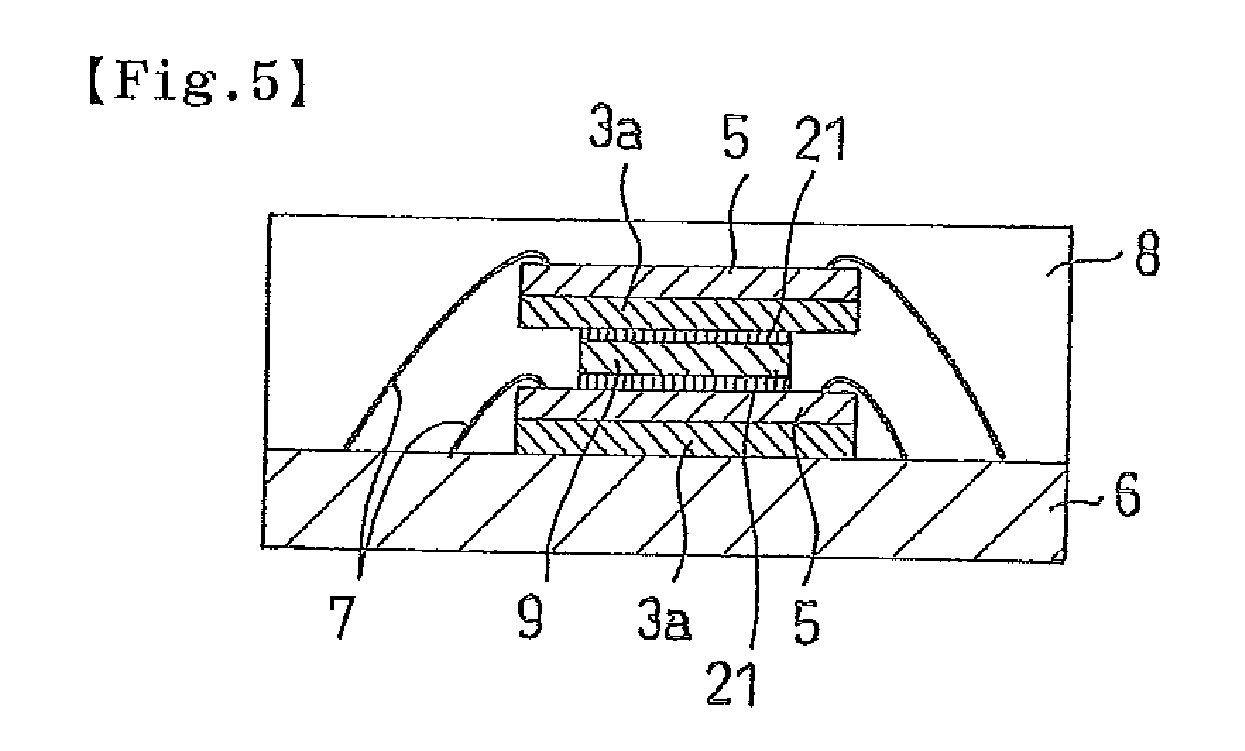
- Description
- Claims
- Application Information
AI Technical Summary
Benefits of technology
Problems solved by technology
Method used
Image

Examples
example 1
[0145]An acrylic polymer A was obtained by charging 95 parts of 2-ethylhexyl acrylate (referred to as “2EHA” in the following), 5 parts of 2-hydroxyethyl acrylate (referred to as “HEA” in the following), and 65 parts of toluene into a reaction vessel equipped with a cooling tube, a nitrogen introducing tube, a thermometer, and a stirrer and polymerizing the contents at 61° C. for 6 hours in a nitrogen air flow.
[0146]Next, a pressure-sensitive adhesive composition solution was produced by adding 3 parts of a polyisocyanate compound (trade name “Colonate L” manufactured by Nippon Polyurethane Industry Co., Ltd.) to 100 parts of the acrylic polymer A.
[0147]A pressure-sensitive adhesive layer having a thickness of 10 μm was formed by applying the pressure-sensitive adhesive composition solution that was prepared as described above onto a polyethylene terephthalate film having a thickness of 50 μm and heat-crosslinking the product at 80° C. for 3 minutes. Next, the obtained pressure-sens...
example 2
[0151]The adhesive film with a dicing sheet according to this example was produced in the same manner as in Example 1 except that the amount of spraying with a silicone spray when modifying the surface of the pressure-sensitive adhesive layer was set so that the intensity of the Si—Kα ray became 100 kcps.
example 3
[0152]The adhesive film with a dicing sheet according to this example was produced in the same manner as in Example 1 except that a silicone resin was transferred onto the surface of the pressure-sensitive adhesive layer (the intensity of the Si—Kα ray on the surface of the pressure-sensitive adhesive layer was 0.9 kcps) using a silicone resin coating film (trade name “Diafoil MRA38” manufactured by Mitsubishi Plastics Inc.) when modifying the surface of the pressure-sensitive adhesive layer.
PUM
| Property | Measurement | Unit |
|---|---|---|
| Temperature | aaaaa | aaaaa |
| Fraction | aaaaa | aaaaa |
| Angle | aaaaa | aaaaa |
Abstract
Description
Claims
Application Information