Method for Fracturing and Forming a Pattern Using Curvilinear Characters with Charged Particle Beam Lithography

a curvilinear character and lithography technology, applied in the field of lithography, can solve the problems of expensive computation time, difficult to accurately translate the physical design to the actual circuit pattern developed on the resist layer, and laborious task of adding opc features

Inactive Publication Date: 2011-03-03
D2S
View PDF24 Cites 40 Cited by
  • Summary
  • Abstract
  • Description
  • Claims
  • Application Information

AI Technical Summary

Problems solved by technology

An example of an end-use limitation is defining the geometry of a transistor in a way in which it cannot sufficiently operate at the required supply voltage.
The design rule limitations reflect, among other things, the smallest dimensions that can be reliably fabricated.
As the critical dimensions of the circuit pattern become smaller and approach the resolution value of the exposure tool, the accurate transcription of the physical design to the actual circuit pattern developed on the resist layer becomes difficult.
Adding OPC features is a very laborious task, requires costly computation time, and results in more expensive reticles.
Not only are OPC patterns complex, but since optical proximity effects are long range compared to minimum line and space dimensions, the correct OPC patterns in a given location depend significantly on what other geometry is in the neighborhood.
There are numerous manufacturing factors that also cause variations, but the OPC component of that overall error is often in the range listed.
Since curvilinear patterns are difficult and expensive to form on a reticle using conventional techniques, rectilinear approximations of the curvilinear patterns may be used.
The cost of charged particle beam lithography is directly related to the time required to expose a pattern on a surface, such as a reticle or wafer.
For the most complex integrated circuit designs, forming the set of layer patterns, either on a set of reticles or on a substrate, is a costly and time-consuming process.

Method used


Image

  • Method for Fracturing and Forming a Pattern Using Curvilinear Characters with Charged Particle Beam Lithography
  • Method for Fracturing and Forming a Pattern Using Curvilinear Characters with Charged Particle Beam Lithography
  • Method for Fracturing and Forming a Pattern Using Curvilinear Characters with Charged Particle Beam Lithography

Examples


Embodiment Construction

[0036]The present disclosure describes generating and exposing a series of curvilinear CP shots to form a continuous track on a surface. A series of shots form a spatial succession, and may be written in any temporal order. Note that the numbers of shots used in the various embodiments illustrated herein are exemplary only, as a series of shots of the present disclosure may number from two or more as desired to achieve the desired target pattern.

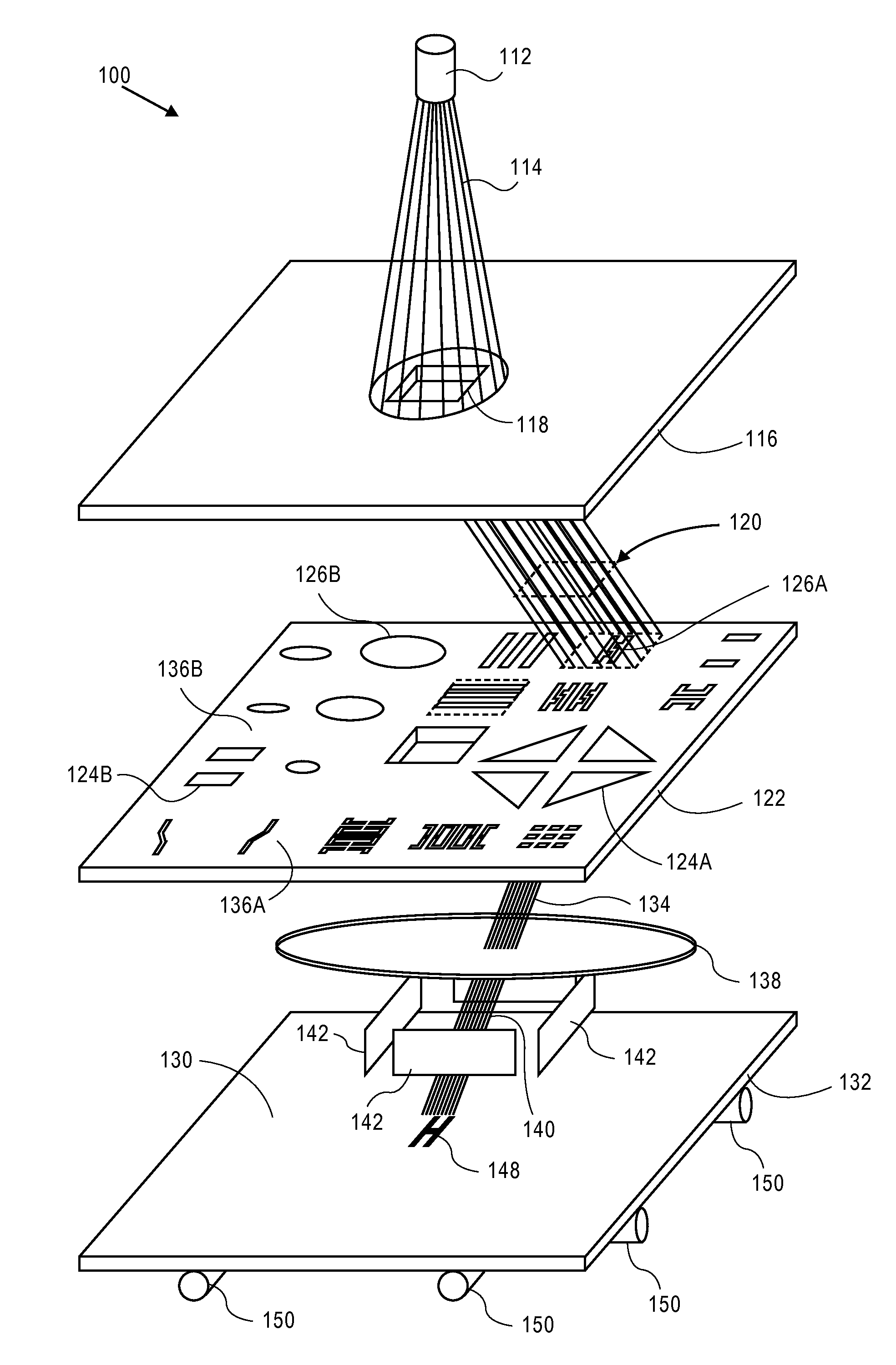
[0037]Referring now to the drawings, wherein like numbers refer to like items, FIG. 1 illustrates an embodiment of a conventional lithography system 100, such as a charged particle beam writer system, in this case an electron beam writer system, that employs character projection to manufacture a surface 130. The electron beam writer system 100 has an electron beam source 112 that projects an electron beam 114 toward an aperture plate 116. The plate 116 has an aperture 118 formed therein which allows the electron beam 114 to pass. Once the el...


PUM

PropertyMeasurementUnit
perimeteraaaaaaaaaa
beam blur radiusaaaaaaaaaa
widthaaaaaaaaaa

Abstract

In the field of semiconductor production using shaped charged particle beam lithography, a method and system for fracturing or mask data preparation or proximity effect correction is disclosed, wherein a series of curvilinear character projection shots are determined for a charged particle beam writer system, such that the set of shots can form a continuous track, possibly of varying width, on a surface. A method for forming a continuous track on a surface using a series of curvilinear character projection shots is also disclosed. Methods for manufacturing a reticle and for manufacturing a substrate such as a silicon wafer by forming a continuous track on a surface using a series of curvilinear character projection shots is also disclosed.

Description

RELATED APPLICATIONS[0001]This application: 1) is a continuation-in-part of U.S. patent application Ser. No. 12 / 603,580 entitled “Method For Fracturing A Pattern For Writing With A Shaped Charged Particle Beam Writing System Using Dragged Shots”, filed on Oct. 21, 2009; and 2) claims priority from U.S. Provisional Patent Application Ser. No. 61 / 237,290 filed Aug. 26, 2009, entitled “Method and System For Manufacturing a Surface Using Charged Particle Beam Lithography”; both of which are hereby incorporated by reference for all purposes.BACKGROUND OF THE DISCLOSURE[0002]The present disclosure is related to lithography, and more particularly to the design of a charged particle beam writer system and methods for using the charged particle beam writer system to manufacture a surface which may be a reticle, a wafer, or any other surface.[0003]In the production or manufacturing of semiconductor devices, such as integrated circuits, optical lithography may be used to fabricate the semicond...

Claims


Application Information

Patent Timeline
Patent Type & Authority Applications(United States)
IPC IPC(8): G03F7/00G06F17/50G03F1/00
CPCB82Y10/00B82Y40/00G03F7/2061H01J37/3026Y10S430/143G03F1/78G03F1/70G06F17/5045H01J37/3174G03F1/36G03F1/68G03F1/20H01L21/0274G06F30/30G06F30/398
Inventor FUJIMURA, AKIRATUCKER, MICHAEL
Owner D2S
Why Eureka
Try Eureka