FinFET Formation with a Thermal Oxide Spacer Hard Mask Formed from Crystalline Silicon Layer

a technology of thermal oxide spacer and hard mask, which is applied in the direction of semiconductor devices, electrical equipment, decorative arts, etc., can solve the problems of non-uniform spacer width, inability to fabricate fin structures with tight or narrow pitches, and inability to control leakage currents

Inactive Publication Date: 2011-03-03
NXP USA INC +1
View PDF3 Cites 60 Cited by
  • Summary
  • Abstract
  • Description
  • Claims
  • Application Information

AI Technical Summary

Problems solved by technology

As semiconductor device scaling continues into the nanoscale regime, the ability to control leakage currents and otherwise develop manufacturable devices becomes more difficult.
While thinner body FinFET devices can be used to obtain more aggressive gate length scaling, to suppress short-channel effects, and to increase the effective channel width by combining multiple fins, the ability to fabricate fin structures with tight or narrow pitches was conventionally limited by capabilities of standard photolithography technologies.
However, there are certain disadvantages with these conventional solutions in terms of pattern fidelity, critical dimension variation, and pattern density that result from non-uniformities in the polysilicon mandrel spacing and line width caused by variations in the trim and etch processes, as well as non-uniformities in the spacer width caused by variations in the spacer formation processes.

Method used


Image

  • FinFET Formation with a Thermal Oxide Spacer Hard Mask Formed from Crystalline Silicon Layer
  • FinFET Formation with a Thermal Oxide Spacer Hard Mask Formed from Crystalline Silicon Layer
  • FinFET Formation with a Thermal Oxide Spacer Hard Mask Formed from Crystalline Silicon Layer

Examples


Embodiment Construction

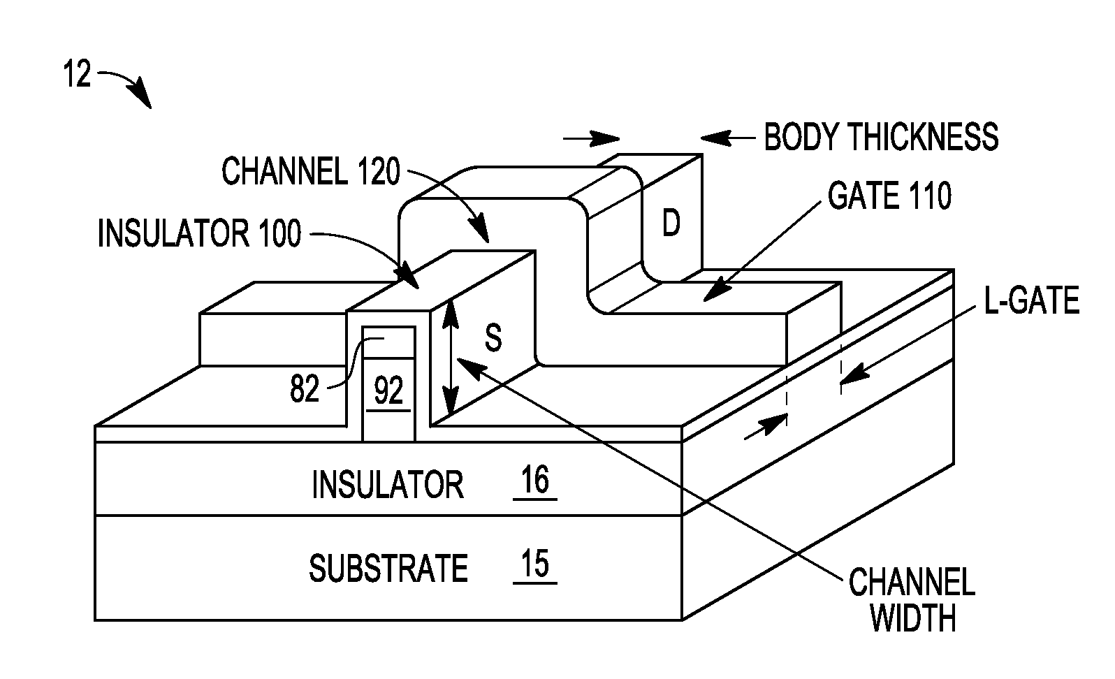
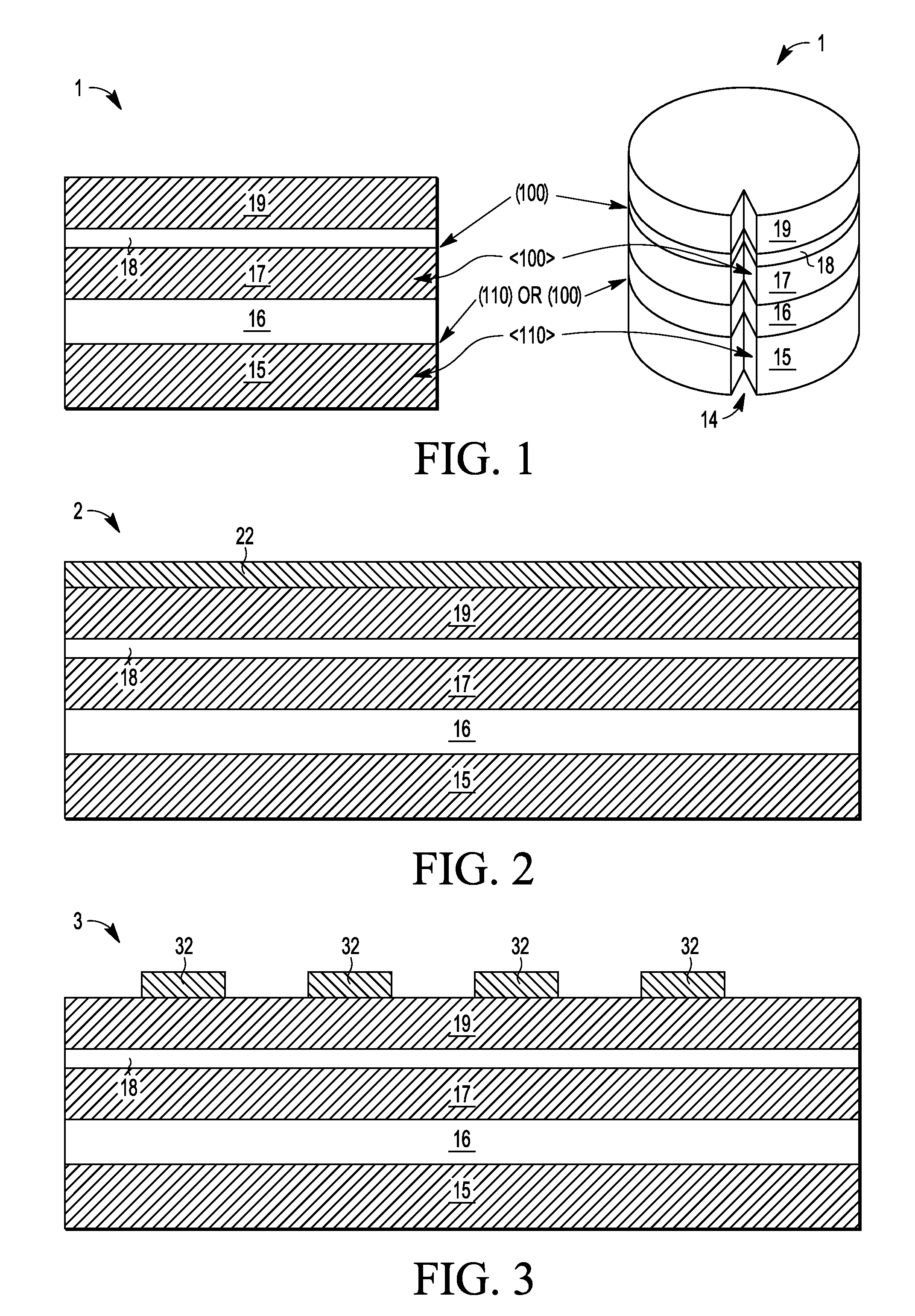
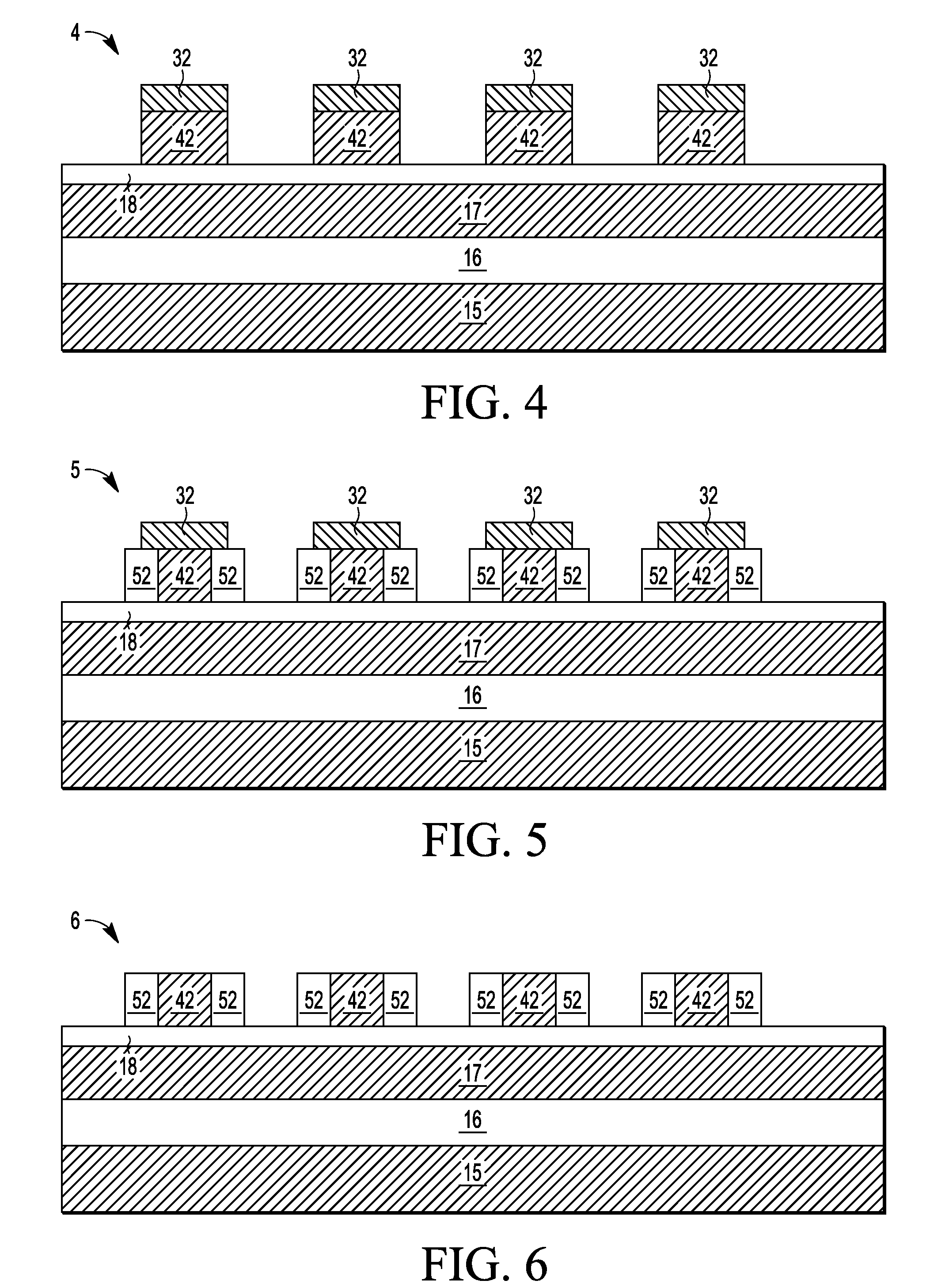
[0020]A method and apparatus are described for fabricating high performance FinFET devices using a double SOI starting substrate where the top SOI semiconductor layer is patterned to form a mandrel of patterned features which are used to pattern the bottom SOI semiconductor layer to form fin structures with tight control of fin pitch and fin thickness. After selectively patterning and trimming the top SOI semiconductor layer to form single crystal dummy structures, the sidewalls of the dummy structures are thermally oxidized to form uniform oxide sidewall spacers. The oxide sidewall spacers remain in place after the remaining dummy structures are removed, and are used as hard mask to pattern the bottom SOI semiconductor layer. By thermally oxidizing the single crystal silicon in the top SOI semiconductor layer, the oxide sidewall spacers can be formed in a controllable and uniform fashion to a desired spacer width to serve as the fin thermal oxide hardmask, thereby reducing fin line...


PUM

PropertyMeasurementUnit
thicknessaaaaaaaaaa
widthaaaaaaaaaa
thicknessaaaaaaaaaa

Abstract

A semiconductor process and apparatus provide a FinFET device by forming a second single crystal semiconductor layer (19) that is isolated from an underlying first single crystal semiconductor layer (17) by a buried insulator layer (18); patterning and etching the second single crystal semiconductor layer (19) to form a single crystal mandrel (42) having vertical sidewalls; thermally oxidizing the vertical sidewalls of the single crystal mandrel to grow oxide spacers (52) having a substantially uniform thickness; selectively removing any remaining portion of the single crystal mandrel (42) while substantially retaining the oxide spacers (52); and selectively etching the first single crystal semiconductor layer (17) using the oxide spacers (52) to form one or more FinFET channel regions (92).

Description

BACKGROUND OF THE INVENTION[0001]1. Field of the Invention[0002]The present invention is directed in general to the field of semiconductor devices. In one aspect, the present invention relates to high-performance field effect transistor devices.[0003]2. Description of the Related Art[0004]As semiconductor device scaling continues into the nanoscale regime, the ability to control leakage currents and otherwise develop manufacturable devices becomes more difficult. Double-gate MOSFET technologies, such as FinFET devices, have been developed to overcome such limitations to transistor scaling. While thinner body FinFET devices can be used to obtain more aggressive gate length scaling, to suppress short-channel effects, and to increase the effective channel width by combining multiple fins, the ability to fabricate fin structures with tight or narrow pitches was conventionally limited by capabilities of standard photolithography technologies. Prior attempts to overcome the limitations of...

Claims


Application Information

Patent Timeline
Patent Type & Authority Applications(United States)
IPC IPC(8): H01L21/3065H01L21/28
CPCH01L21/3086H01L29/66795H01L21/845
Inventor MURALIDHAR, RAMACHANDRANKHATER, MARWAN H.
Owner NXP USA INC
Why Eureka
Try Eureka