Epitaxial wafer, light-emitting element, method of fabricating epitaxial wafer and method of fabricating light-emitting element

a technology of epitaxial wafer and light-emitting element, which is applied in the direction of semiconductor/solid-state device manufacturing, electrical apparatus, semiconductor devices, etc., can solve the problems of reducing affecting the production efficiency of semiconductors, and difficult to improve the light-emitting output without thickening the optical reflective layer, etc., to achieve low forward voltage, increase the manufacturing cost, and high output

Inactive Publication Date: 2011-03-10
SUMITOMO CHEM CO LTD
View PDF4 Cites 4 Cited by
  • Summary
  • Abstract
  • Description
  • Claims
  • Application Information

AI Technical Summary

Benefits of technology

[0058]An epitaxial wafer, a light-emitting element, a method of fabricating the epitaxial wafer, and a method of fabricating the light-emitting element according to this invention can provide an epitaxial wafer and a light-emitting element with a high output and a low forward voltage, and methods of fabricating the epitaxial wafer and the light-emitting element without largely increasing the fabricating cost.

Problems solved by technology

In the light-emitting element described in JP-A 5-37017, however, it is difficult to improve the light-emitting output without thickening the optical reflective layer, though it is possible to widen a wavelength width of the reflected light in the optical reflective layer itself.
In such a case, there is a concern that a fabricating cost largely rises up because of the increases of raw materials and the growth time according to the increase of the number of the total layers to be grown up.
Furthermore, there is a case that it is impossible to improve largely the light-emitting out even in the light-emitting element comprising both the conventional optical reflective layer and the convexoconcave portion on the surface of the element.

Method used


Image

  • Epitaxial wafer, light-emitting element, method of fabricating epitaxial wafer and method of fabricating light-emitting element
  • Epitaxial wafer, light-emitting element, method of fabricating epitaxial wafer and method of fabricating light-emitting element
  • Epitaxial wafer, light-emitting element, method of fabricating epitaxial wafer and method of fabricating light-emitting element

Examples


first embodiment

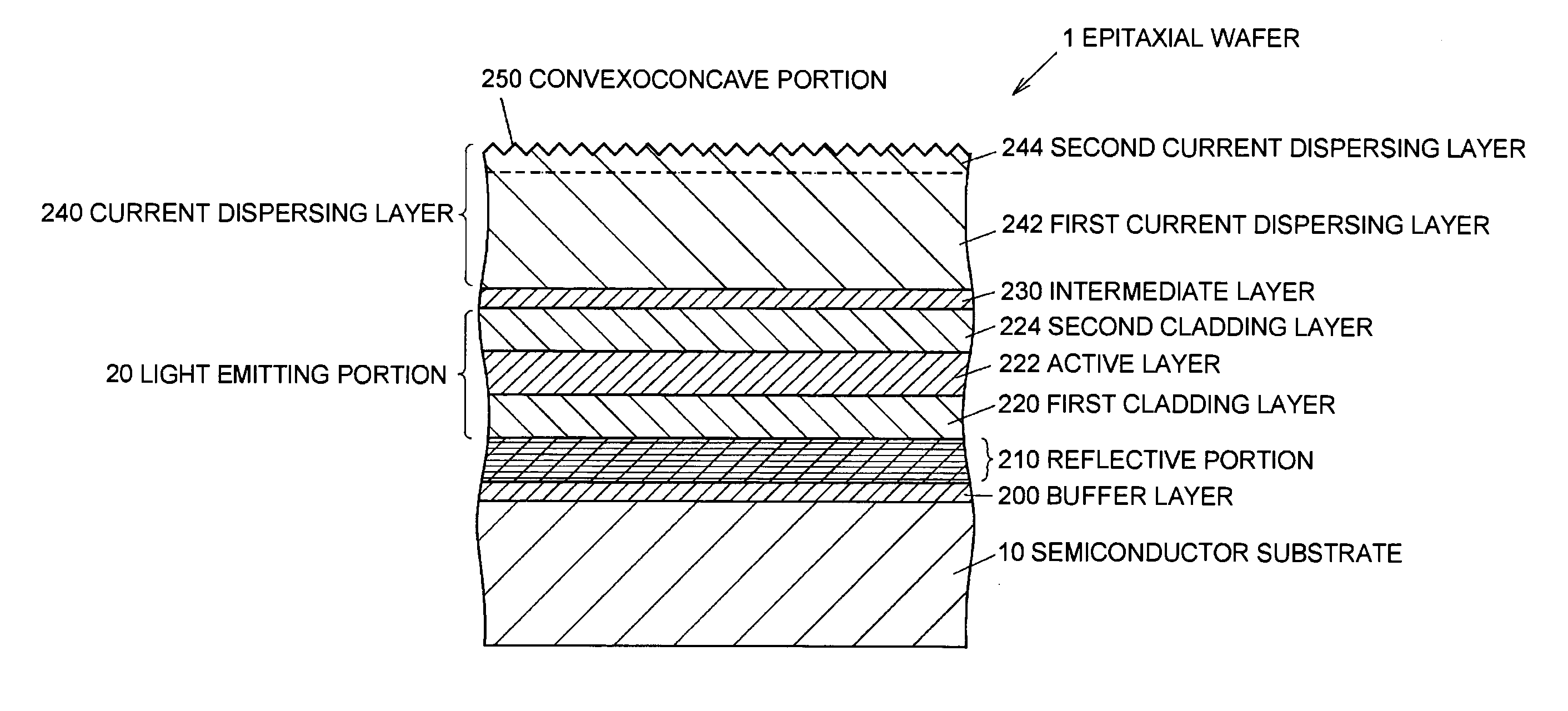
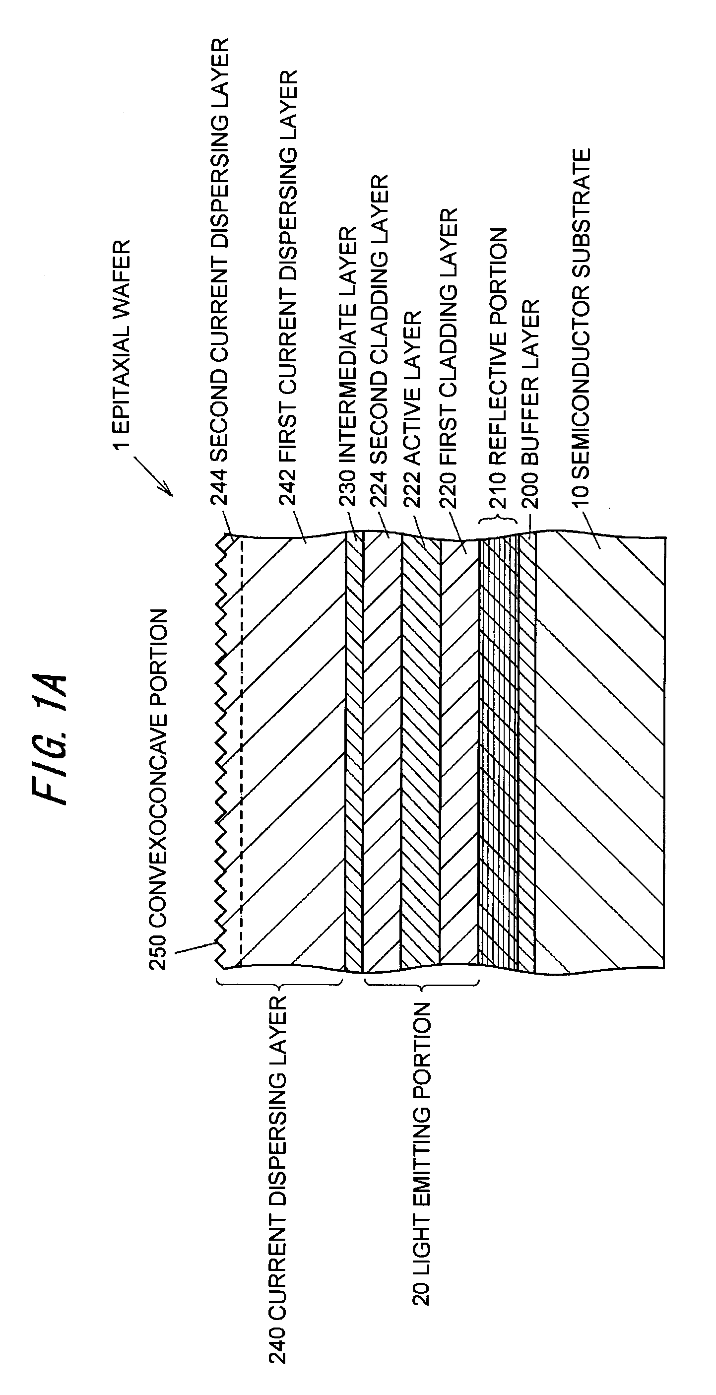
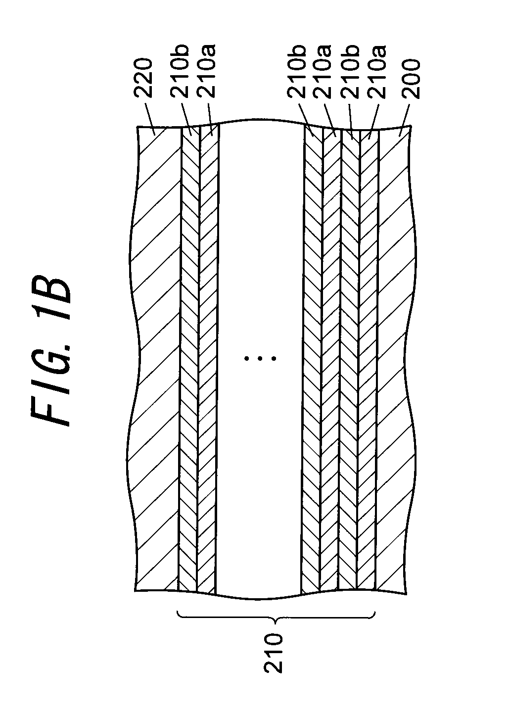
[0095]FIG. 1A shows a schematic partial cross section of an epitaxial wafer of a first embodiment of the invention and FIG. 1B shows a schematic cross section of a reflective portion composing the epitaxial wafer of the first embodiment of the invention.

(Structural Overview of Epitaxial Wafer 1)

[0096]The epitaxial wafer 1 of the first embodiment is, for example, for a light-emitting diode (hereinafter LED) as a semiconductor light-emitting element for emitting red light. The epitaxial wafer 1 concretely comprises an n-type semiconductor substrate 10 of a first conductivity type, an n-type buffer layer 200 provided on the semiconductor substrate 10, a reflective portion 210 including a multi-layers of n-type compound semiconductor provided on the buffer layer 200, an n-type first cladding layer 220 provided on the reflective portion 210, an active layer 222 provided on the first cladding layer 220, a p-type second cladding layer 224 of a second conductivity type different from the fi...

second embodiment

[0123]FIG. 2A shows a schematic cross sectional view of a light-emitting element of a second embodiment of this invention, and the FIG. 2B shows a schematic plan view of the light-emitting element of the second embodiment of this invention.

[0124]The light-emitting element 2 of the second embodiment is formed from the epitaxial wafer 1 of the first embodiment and comprises substantially the same structure as the epitaxial wafer 1 except for a construction having a front surface electrode 30 and a back surface electrode 35. Therefore, explanation in detail is omitted except for the difference.

(Structural Outline of Light-Emitting Element 2)

[0125]A light-emitting element 2 of a second embodiment comprises a semiconductor substrate 10, a reflective portion 210 on the semiconductor substrate 10, a first cladding layer 220 on the reflective portion 210, an active layer 222 on the first cladding layer 220, a second cladding layer 224 on the active layer 222, an intermediate layer 230 on th...

first and second embodiments

(Advantage of First and Second Embodiments)

[0132]The light-emitting element 2 fabricated from the epitaxial wafer 1 in the first embodiment comprises the reflective portion comprising plural pairs of layers including the first semiconductor layer 210a and the second semiconductor layer 210b, a thickness of which are controlled correspondingly to various thickness controlled for the plural incident angles. According to this structure, the reflective portion 210 can reflect the light to the light-extracting side, even if the light enters to the reflective portion 210 with various angles. Furthermore, the light-emitting element 2 comprises the convexoconcave portion 250 at the light-extracting side. Therefore, the light reflected from the reflective portion 210 may be extracted effectively. Accordingly, it is possible to provide the light-emitting element 2 of this embodiment which is improved in the light-extracting efficiency.

[0133]Furthermore, in the light-emitting element 2 fabrica...


PUM


Abstract

An epitaxial wafer, a light-emitting element, a method of fabricating the epitaxial wafer and a method of fabricating the light-emitting element, which have a high output and a low forward voltage, and can be fabricated without increasing fabricating cost, are provided. The epitaxial wafer is formed with a light-emitting portion, a reflective portion provided between a semiconductor substrate and the light-emitting portion and a current dispersing layer having first and second current dispersing layers, wherein the reflective portion has plural pairs of layers having first and second semiconductor layers wherein the first semiconductor layer has a thickness of TA defined by Equation (1),
TA=λp4nA1-(nInsinθnA)2(1)
the second semiconductor layer has a thickness of TB defined by Equation (2),
TB=λp4nB1-(nInsinθnB)2(2)
and the second current dispersing layer has a high carrier density or a high impurity density and is provided with the convexoconcave portion on the surface.

Description

[0001]The present application is based on Japanese Patent Application No. 2009-204289 filed on Sep. 4, 2009, the entire contents of which are incorporated herein by reference.BACKGROUND OF THE INVENTION[0002]1. Field of the Invention[0003]The present invention relates to an epitaxial wafer, a light-emitting element, a method of fabricating the epitaxial wafer and a method of fabricating the light-emitting element. Especially, the present invention relates to an epitaxial wafer and a light-emitting element comprising a convexoconcave portion (an irregularity portion) on a light-extracting surface and a reflective layer comprising plural semiconductor layers, a method of fabricating the epitaxial wafer and a method of fabricating the light-emitting element.[0004]2. Related Art[0005]A conventional light-emitting element comprising an n-type GaAs substrate, an optical reflective layer on the n-type GaAs substrate, an n-type Al0.45Ga0.55As cladding layer on the optical reflective layer, ...

Claims


Application Information

Patent Timeline
Patent Type & Authority Applications(United States)
IPC IPC(8): H01L33/00
CPCH01L33/22H01L33/10
Inventor KONNO, TAICHIROO
Owner SUMITOMO CHEM CO LTD
Why Eureka
Try Eureka