Ultra high voltage mos transistor device

a high-voltage mos transistor and high-voltage technology, applied in the direction of transistors, semiconductor devices, electrical equipment, etc., can solve the problem of higher ron and suffer the effect of higher breakdown voltage of ldmos transistor devices, and improve the formation of fully-depleted regions

Active Publication Date: 2011-03-10
UNITED MICROELECTRONICS CORP
View PDF8 Cites 51 Cited by
  • Summary
  • Abstract
  • Description
  • Claims
  • Application Information

AI Technical Summary

Benefits of technology

[0013]According to the ultra high voltage MOS transistor device provided by the present invention, the recessed channel region is provided to alleviate the large curvature problem of the potential lines occurred at the channel region, the first doped region is provided to preven...

Problems solved by technology

However, this method suffers higher RON due t...

Method used


Image

  • Ultra high voltage mos transistor device
  • Ultra high voltage mos transistor device
  • Ultra high voltage mos transistor device

Examples


Embodiment Construction

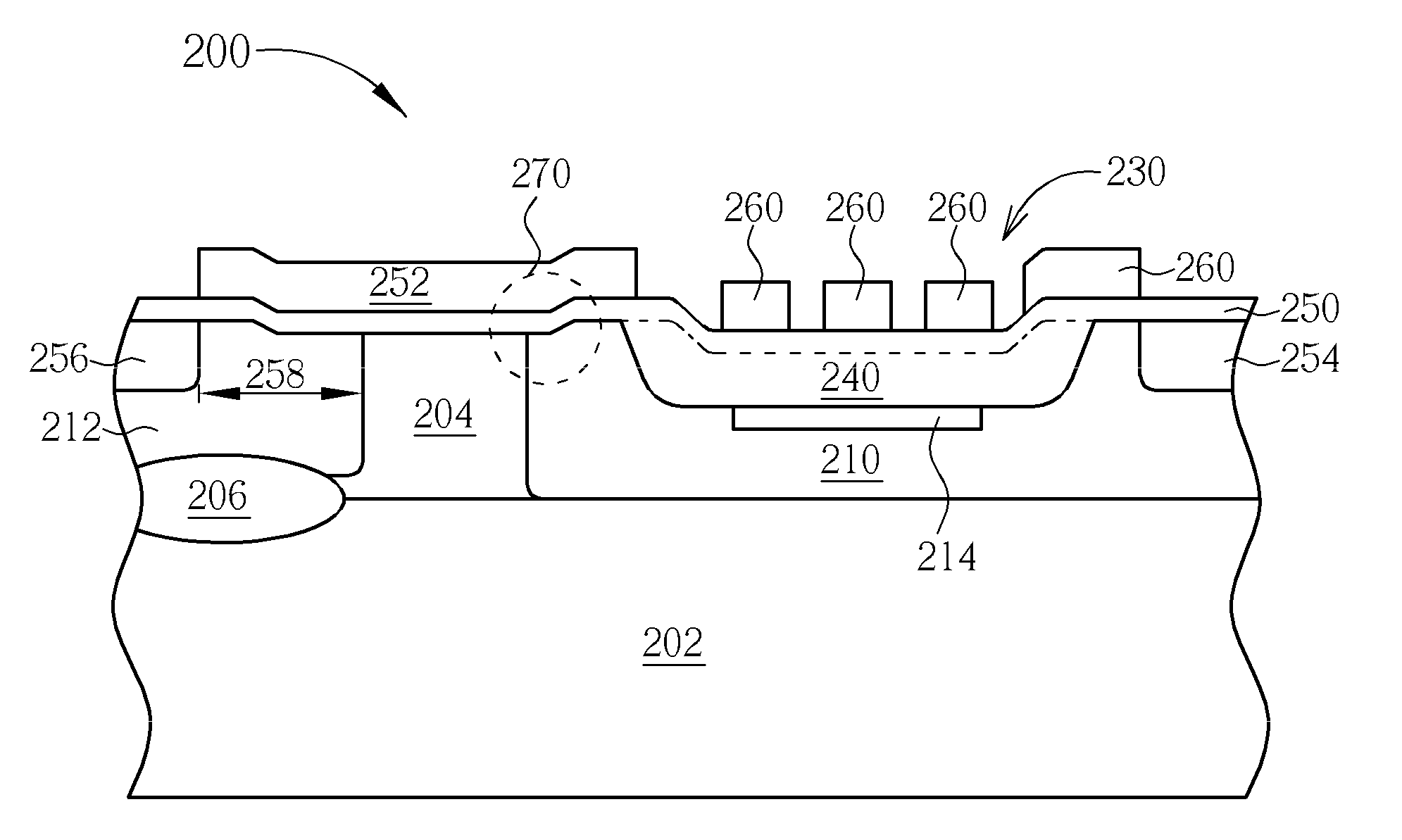
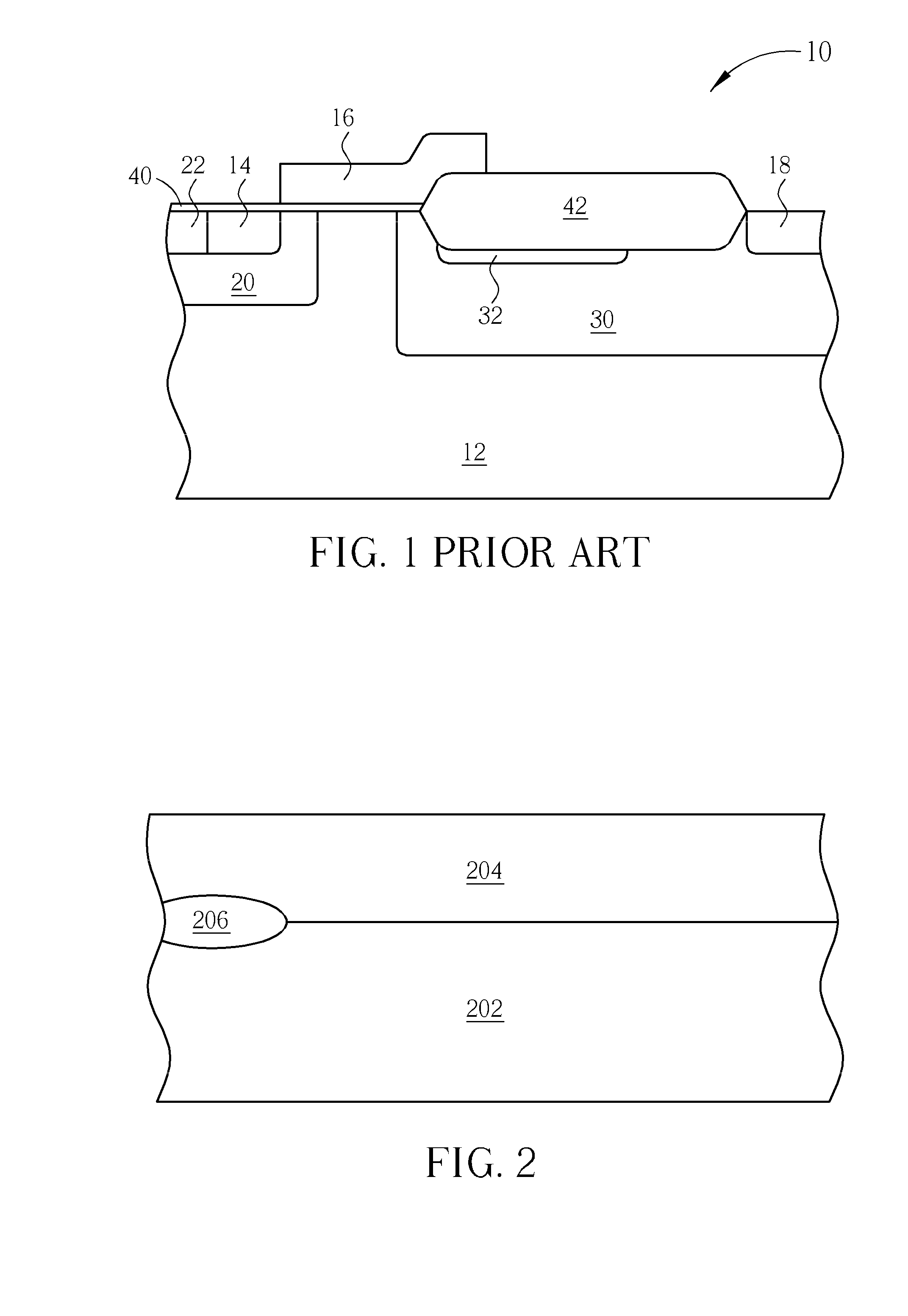
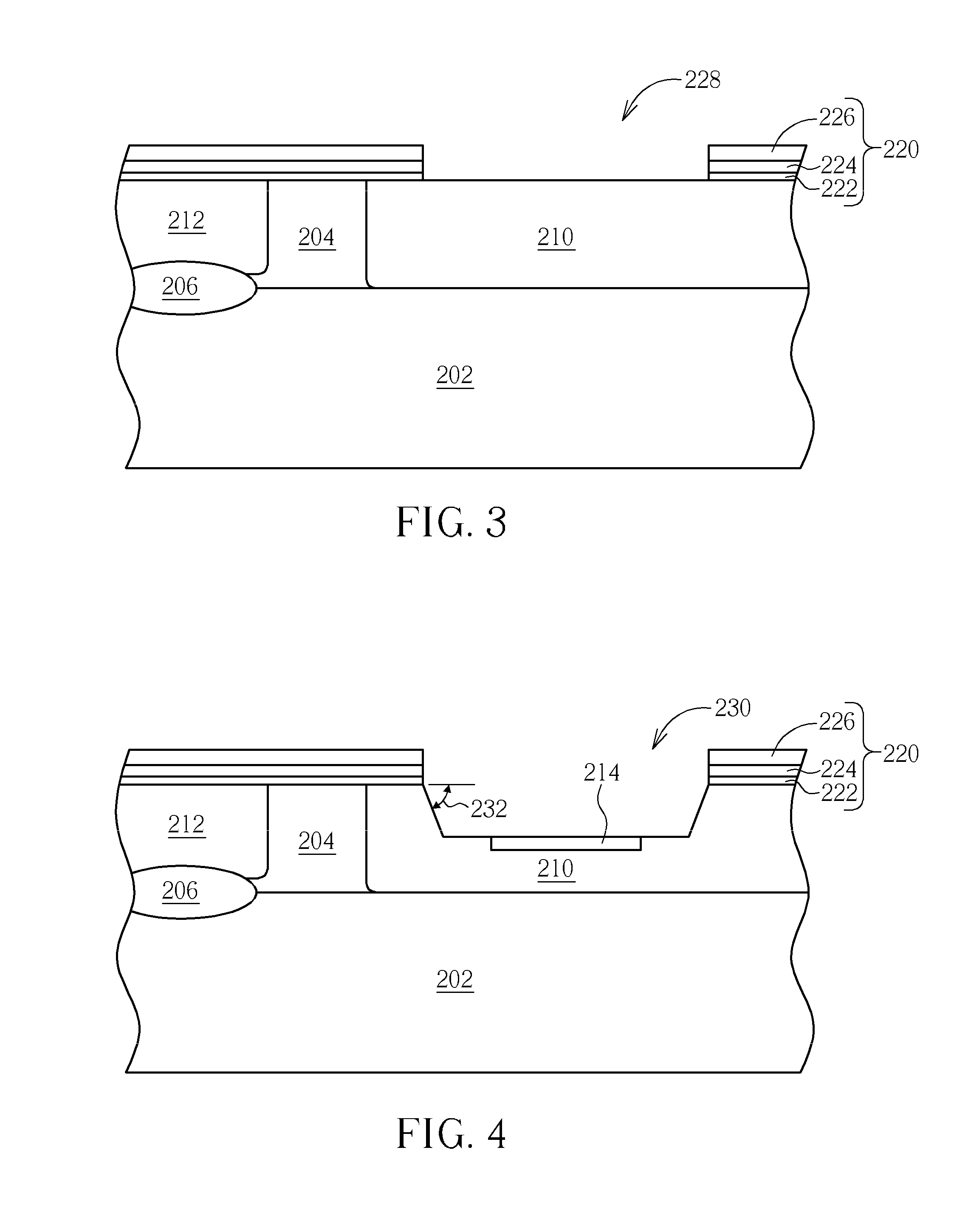
[0017]Please refer to FIGS. 2-8, which are cross-sectional view illustrating formation of an ultra high voltage MOS transistor device provided by a preferred embodiment of the present invention. In this preferred embodiment, the first conductive type is P-type and the second conductive type is N-type. However, it is well-known to those skilled in the art that the first conductive type and the second conductive type can respectively be N-type and P-type. As shown in FIG. 2, the ultra high voltage MOS transistor device provided by the present invention is fabricated on a semiconductor substrate having the first conductive type, such as a P-type substrate 202, and is electrically isolated from other devices by at least a field oxide layer or a shallow trench isolation (STI) (not shown). Next, P-type dopants are implanted into the P-type substrate 202 by an ion implantation and followed by forming an epitaxial layer having the second conductive type, such as an N-type epitaxial layer 20...


PUM


Abstract

An ultra high voltage MOS transistor device includes a substrate having a first conductive type, a first well having a second conductive type and a second well having the first conductive type formed in the substrate, a drain region having the second conductive type formed in the first well, a source region having the second conductive type formed in the second well, a first doped region having the first conductive type formed between the second well and the substrate, an insulating layer formed in a first recess in the first well, a gate formed on the substrate between the source region and the first well, and a recessed channel region formed in the substrate underneath the gate.

Description

BACKGROUND OF THE INVENTION[0001]1. Field of the Invention[0002]The present invention relates to an ultra high voltage MOS transistor device, and more particularly, to an ultra high voltage lateral double-diffused metal-oxide-semiconductor (LDMOS) transistor device.[0003]2. Description of the Prior Art[0004]Double-diffused MOS (DMOS) transistor devices have drawn much attention in power devices having high voltage capability. The conventional DMOS transistor devices are categorized into vertical double-diffused MOS (VDMOS) transistor device and lateral double-diffused MOS (LDMOS) transistor device. Having advantage of higher operational bandwidth, higher operational efficiency, and convenience to be integrated with other integrated circuit due to its planar structure, LDMOS transistor devices are widely used in high operational voltage environment such as CPU power supply, power management system, AC / DC converter, and high-power or high frequency (HF) band power amplifier. The essen...

Claims


Application Information

Patent Timeline
IPC IPC(8): H01L29/78
CPCH01L29/66704H01L29/7816H01L29/0878H01L29/0634H01L29/1037H01L29/0653H01L29/1095H01L29/404
Inventor TANG, SUNG-NIENYANG, SHENG-HSIONG
Owner UNITED MICROELECTRONICS CORP
Why Eureka
Try Eureka