Organic electroluminescence display device

a display device and organic technology, applied in the direction of organic semiconductor devices, semiconductor devices, instruments, etc., can solve the problems of difficult manufacture of decreased light taken out of the top side of the organic electroluminescence display devices, and so as to reduce the electric resistance of the upper electrode and make the disconnection of the upper electrode scarcely occur

Active Publication Date: 2011-03-10
JAPAN DISPLAY INC +1
View PDF5 Cites 59 Cited by
  • Summary
  • Abstract
  • Description
  • Claims
  • Application Information

AI Technical Summary

Benefits of technology

The present invention has been made to overcome the above-mentioned drawbacks, and it is an object of the present invention to provide an organic electroluminescence display device which can decrease the electric resistance of an upper electrode while maintaining required light transmission quantity by using a thin silver film in forming the upper electrode, and can make the disconnection of the upper electrode scarcely occur between a power source part and a display region.
According to the present invention, it is possible to provide the organic electroluminescence display device which can decrease the electric resistance of the upper electrode while maintaining required light transmission quantity by using the thin silver film in forming the upper electrode, and can make the disconnection of the upper electrode scarcely occur between the power source part and the display region.

Problems solved by technology

However, silver exhibits high aggregation property and hence, when a silver layer is formed into a thin film shape, there arises a case where the disconnection of an upper electrode occurs.
On the other hand, for example, when a thickness of the silver layer is increased to make the occurrence of the disconnection difficult, a quantity of light which is taken out of a top side of the organic electroluminescence display device is decreased.
Further, depending on a kind of impurity or an addition quantity of impurity, an optical characteristic or an electric characteristic changes sensitively thus making the manufacture of the organic electroluminescence display device difficult.

Method used


Image

  • Organic electroluminescence display device
  • Organic electroluminescence display device
  • Organic electroluminescence display device

Examples


first embodiment

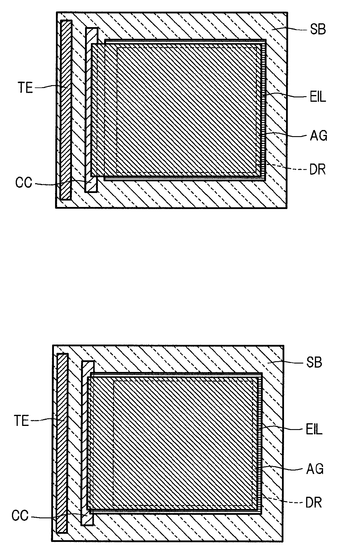
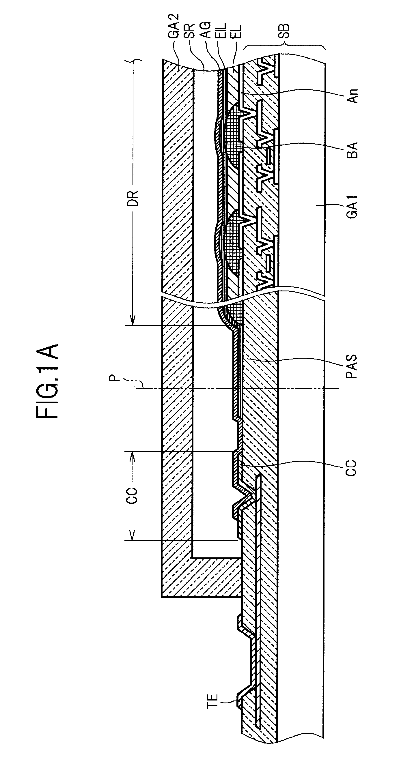
An organic electroluminescence display device according to a first embodiment of the present invention is a top-emission type organic electroluminescence display device which is constituted of a TFT substrate which is formed by arranging organic electroluminescence elements on a glass substrate in a matrix array and a sealing substrate which is laminated to the TFT substrate and seals a region where the organic electroluminescence elements are arranged, wherein a display region on which an image is displayed is formed over a sealing substrate side.

On the TFT substrate, a large number of scanning signal lines are mounted at an equal interval from each other and, at the same time, a large number of video signal lines are mounted at an equal interval from each other in the direction perpendicular to the direction that the scanning signal lines are mounted. In each of pixel regions defined by these scanning signal lines and the video signal lines, a thin film transistor having the MIS (...

second embodiment

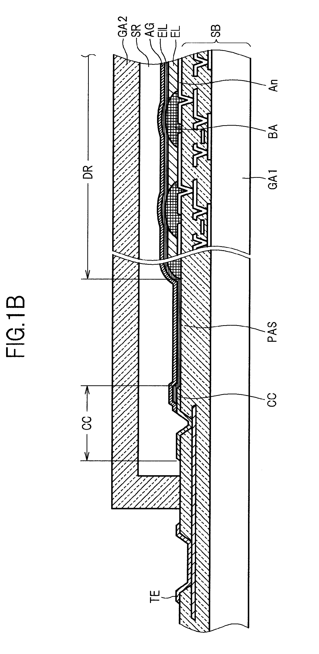
Next, the second embodiment of the present invention is explained. FIG. 3 shows a cross section of an organic electroluminescence display device according to the second embodiment. In the second embodiment, in each of a plurality of pixels formed in a display region DR, an electron transport layer ETL is arranged between an organic film EL and a thin silver film AG, and the electron transport layer ETL is made of an organic material having electron transportability which includes an electron pair donor. Particularly, in the second embodiment, a background layer of the thin silver film AG formed between the display region DR and a power source part CC is formed using the same material as the electron transport layer ETL thus suppressing aggregation property of the thin silver film AG. The organic electroluminescence display device according to the second embodiment and the organic electroluminescence display device according to the first embodiment have substantially the same constit...

third embodiment

FIG. 4 shows a cross section of an organic electroluminescence display device according to the third embodiment. In the first embodiment and the second embodiment, a background layer made of the same material as the electron injection layer EIL or the electron transport layer ETL is formed over the background of at least the portion of the thin silver film AG between the display region DR and the power source part CC. The third embodiment differs from the first and second embodiments with respect to a point that a background layer of a thin silver film AG between a display region DR and a power source part CC is formed of a protective layer PASV having an electron pair donor.

To be more specific, the protective layer PASV is formed by forming a polyimide film and by applying ultraviolet treatment to the polyimide film. It is thought that polyimide becomes an electron pair donor due to such ultraviolet treatment so that the aggregation of the thin silver film AG is suppressed. The rea...


PUM


Abstract

In an organic electroluminescence display device which includes: a display region DR in which a plurality of pixels are arranged; and a power source part CC which is arranged outside the display region, each of the plurality of pixels includes: a lower electrode An; a light emitting layer stacked above the lower electrode; and an upper electrode which includes a thin silver film AG and is formed by a layer shared in common by other pixels above the light emitting layer, the upper electrode extends to the power source part for electrically connection, the thin silver film has a portion arranged between the display region and the power source part, and a background layer containing an electron pair donor is arranged as a background of at least a portion of the thin silver film between the display region and the power source part.

Description

CROSS-REFERENCE TO RELATED APPLICATIONSThe present application claims priority from Japanese applications JP 2009-204981 filed on Sep. 4, 2009, and JP 2010-178791 filed on Aug. 9, 2010, the contents of which are hereby incorporated by reference into this application.BACKGROUND OF THE INVENTION1. Field of the InventionThe present invention relates to a top-emission-type organic electroluminescence display device.2. Description of the Related ArtIn a top-emission-type organic electroluminescence display device which uses organic light emitting elements (OLED: Organic Light Emitting Diodes), there is a case where a silver layer stacked like a thin film is used for decreasing the electric resistance of an upper electrode which supplies a potential to a light emitting layer of each organic light emitting element. Although silver is a material which absorbs light little and possesses high reflectance, by stacking a thin-film-like silver layer above the light emitting layer, light can be t...

Claims


Application Information

Patent Timeline
Patent Type & Authority Applications(United States)
IPC IPC(8): G09G3/30G09G5/00
CPCH01L27/3246H01L27/3258H01L27/3276H01L2251/5315H01L51/5092H01L51/5234H01L51/5246H01L51/5048H10K59/124H10K59/122H10K59/131H10K50/14H10K50/171H10K50/828H10K50/8426H10K2102/3026
Inventor MATSUURA, TOSHIYUKIYAMAGUCHI, HIROHITOYOSHIDA, MASANORIMIZUNO, NOBUTAKAOYA, KATSUNORI
Owner JAPAN DISPLAY INC
Why Eureka
Try Eureka