Nitride semiconductor substrate, semiconductor device, and methods for manufacturing nitride semiconductor substrate and semiconductor device

Active Publication Date: 2011-03-24
SUMITOMO ELECTRIC IND LTD
View PDF5 Cites 17 Cited by
  • Summary
  • Abstract
  • Description
  • Claims
  • Application Information

AI Technical Summary

Benefits of technology

[0006]The present invention has been made in order to solve the above-described problems, and an object of the present invention is to provide a nitride semiconductor substrate having a main surface serving as a semipolar plane and provided with a c

Problems solved by technology

However, Japanese Patent Laying-Open No. 2004-319951 as described above discloses a substrate having a main surface corresponding to the c-plane, b

Method used


Image

  • Nitride semiconductor substrate, semiconductor device, and methods for manufacturing nitride semiconductor substrate and semiconductor device
  • Nitride semiconductor substrate, semiconductor device, and methods for manufacturing nitride semiconductor substrate and semiconductor device
  • Nitride semiconductor substrate, semiconductor device, and methods for manufacturing nitride semiconductor substrate and semiconductor device

Examples


first embodiment

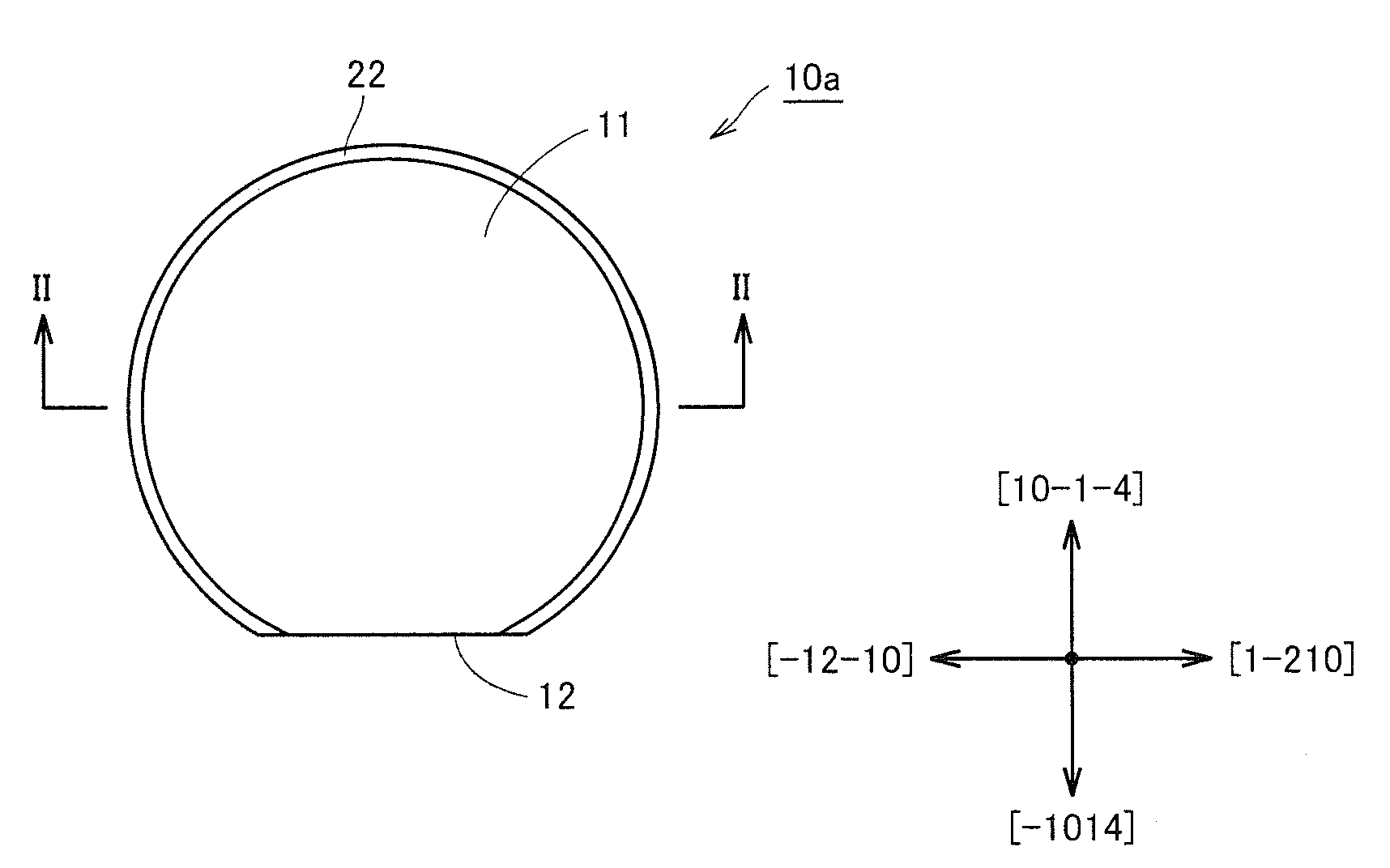
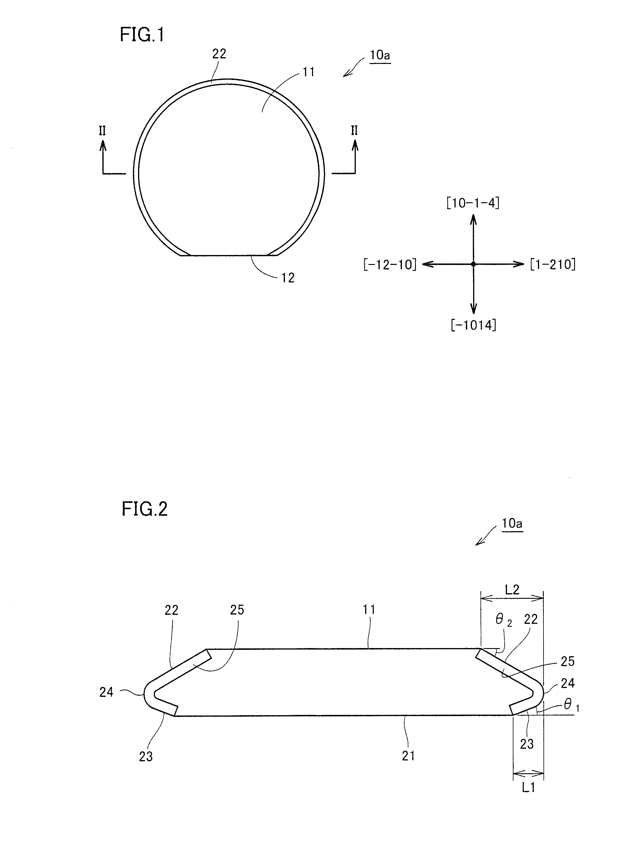
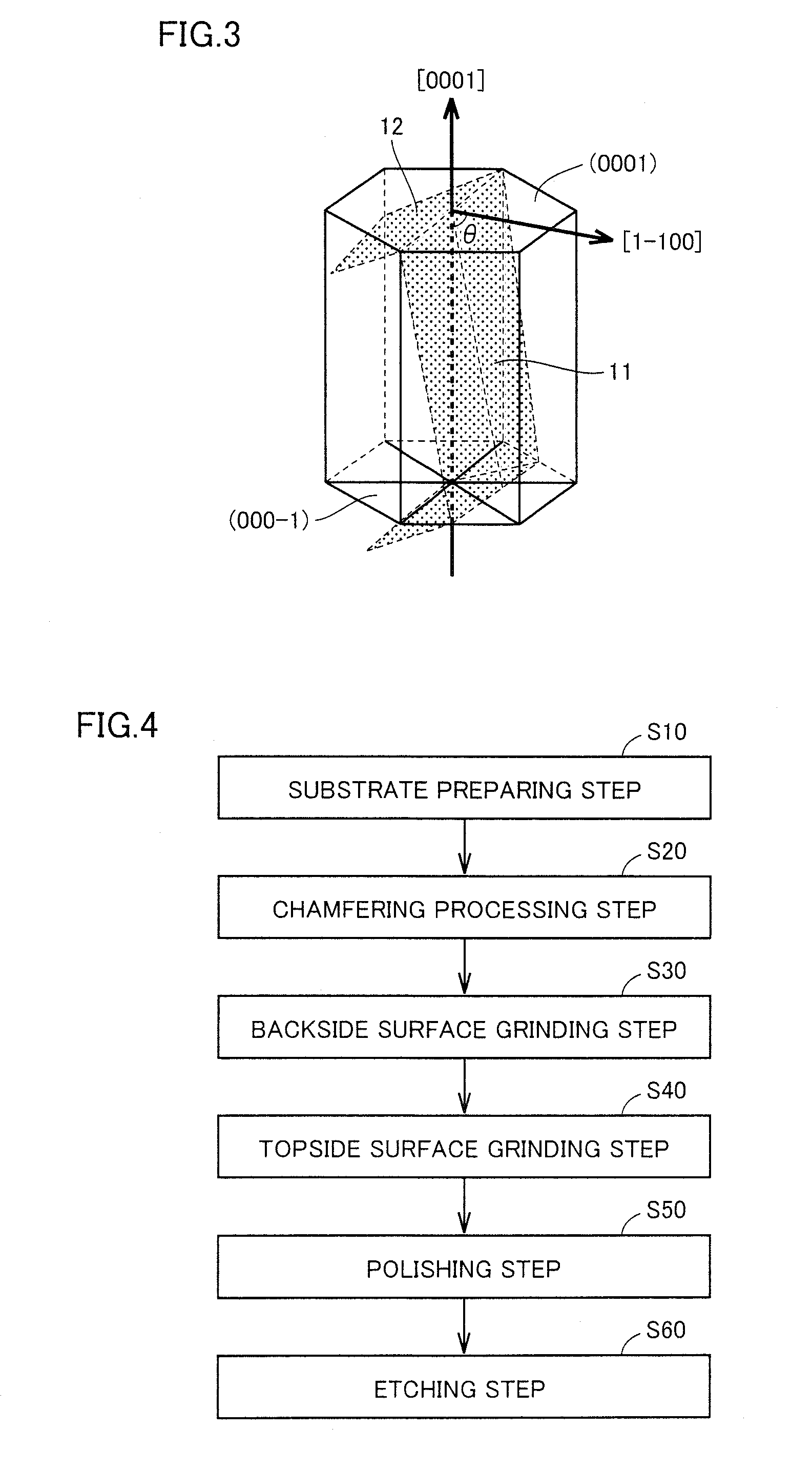
[0036]Referring to FIGS. 1-3, the first embodiment of the nitride semiconductor substrate according to the present invention will be hereinafter described.

[0037]As shown in FIGS. 1 and 2, a nitride semiconductor substrate 10a according to the present invention has an approximately circular shape as seen in plan view and has an orientation flat 12 formed by linearly processing a part of the edge of the outer periphery. Furthermore, on the edge of the outer periphery of nitride semiconductor substrate 10a, a topside chamfer 22 is formed which corresponds to a chamfered portion located on the main surface 11 side. Furthermore, on the outer periphery of a backside surface 21 on the side opposite to main surface 11, a backside chamfer 23 is formed which corresponds to a chamfered portion located on the backside surface 21 side. At the edge of the outer periphery of nitride semiconductor substrate 10a, an edge face 24 having a curved surface is formed so as to connect topside chamfer 22 a...

second embodiment

[0110]Referring to FIGS. 18 and 19, a light emitting element fabricated using the nitride semiconductor substrate according to the present invention will then be described.

[0111]Referring to FIG. 18, the light emitting element includes a nitride semiconductor substrate 10a corresponding to a GaN substrate of n-type conductivity, an n-type GaN layer 41, an AlGaN layer 42 formed on n-type GaN layer 41, a light emitting layer 43 formed on AlGaN layer 42, a p-type AlGaN layer 44 formed on light emitting layer 43, and a p-type GaN layer 45 formed on p-type AlGaN layer 44. Nitride semiconductor substrate 10a which is an n-type GaN substrate exhibits characteristics, for example, having a resistance value of 1×10⁻² Ωcm and a concentration of the n-type conductive impurities of 3×10¹⁸ / cm3. For example, n-type GaN layer 41 can be configured to have a thickness of 1 μm. Furthermore, silicon (Si) can be used as conductive impurities contained in this n-type GaN layer. For example, n-type AlGaN...

example 1

[0146]In this example, the usability of the GaN substrate cut out from the (0001) GaN ingot in the [1-100] direction at an angle θ in the range between 68° and 82° was examined (Test 1). Specifically, the substrate with an angle different from angle θ was used to form an element of a semiconductor laser device and measure the oscillation yield of the element. Furthermore, an examination was made with regard to the effects of the inclination angle (θ1 or θ2) of the chamfered portion with respect to adjacent one of main surface 11 and backside surface 21 on the side opposite to main surface 11 (Test 2).

[0147](Test 1)

[0148]Preparation of Sample

[0149]First, the (0001) GaN ingot thickly grown by the HVPE method was cut at an angle θ in the range between 68° and 82° in the [1-100] direction using a wafer slicing apparatus to fabricate a GaN substrate (sample IDs in Table 1 set forth below: I-1 to I-9) in which an inclination angle θ formed between the [0001] direction and the [1-100] dire...


PUM

PropertyMeasurementUnit
Thicknessaaaaaaaaaa
Thicknessaaaaaaaaaa
Angleaaaaaaaaaa

Abstract

A nitride semiconductor substrate having a main surface serving as a semipolar plane and provided with a chamfered portion capable of effectively preventing cracking and chipping, a semiconductor device fabricated using the nitride semiconductor substrate, and a method for manufacturing the nitride semiconductor substrate and the semiconductor device are provided. The nitride semiconductor substrate includes a main surface inclined at an angle of 71° or more and 79° or less with respect to the (0001) plane toward the [1-100] direction or inclined at an angle of 71° or more and 79° or less with respect to the (000-1) plane toward the [−1100] direction; and a chamfered portion located at an edge of an outer periphery of the main surface. The chamfered portion is inclined at an angle θ1 or θ2 of 5° or more and 45° or less with respect to adjacent one of the main surface and a backside surface on a side opposite to the main surface. Accordingly, cracking and chipping occurring from the edge of the outer periphery of the nitride semiconductor substrate can be effectively suppressed.

Description

BACKGROUND OF THE INVENTION[0001]1. Field of the Invention[0002]The present invention relates to a nitride semiconductor substrate, a semiconductor device and methods for manufacturing the nitride semiconductor substrate and the semiconductor device, and more particularly to a nitride semiconductor substrate having a main surface serving as a semipolar plane, a semiconductor device, and methods for manufacturing the nitride semiconductor substrate and the semiconductor device.[0003]2. Description of the Background Art[0004]A nitride semiconductor substrate such as a GaN substrate having an energy band gap of 3.4 eV and a high thermal conductivity has been attracting attention as material for a semiconductor device such as a power electronic device and an optical device of a short wavelength. In order to prevent chipping, cracking and the like of the substrate, it is proposed to provide a chamfered portion at the edge of the outer periphery in the GaN substrate which is an example of...

Claims


Application Information

Patent Timeline
IPC IPC(8): H01L29/205H01L21/20B26D1/00
CPCC30B29/406H01L21/02021C30B33/00Y10T83/04
Inventor YAMAGUCHI, SAYURIMATSUMOTO, NAOKIMIKAMI, HIDENORI
Owner SUMITOMO ELECTRIC IND LTD
Why Eureka
Try Eureka