Semiconductor apparatus and method of detecting characteristic degradation of semiconductor apparatus

a semiconductor and characteristic degradation technology, applied in the field of semiconductor apparatus and characteristic degradation detection of semiconductor apparatus, can solve the problems of power mosfet breakdown power mosfet breakdown, etc., and achieve the effect of preventing a failure of the semiconductor apparatus

Active Publication Date: 2011-03-24
RENESAS ELECTRONICS CORP
View PDF8 Cites 26 Cited by
  • Summary
  • Abstract
  • Description
  • Claims
  • Application Information

AI Technical Summary

Benefits of technology

[0039]Because the method of detecting characteristic degradation of a semiconductor apparatus according to the exemplary aspect of the present invention can detect characteristic degradation which leads to a failure of the semiconductor apparatus based on a set value determined based on an initial characteristic value of the semiconductor apparatus and a characteristic value of the semiconductor apparatus at given timing, it is possible to prevent a failure of the semiconductor apparatus from occurring.
[0040]According to the exemplary aspects of the present invention described above, it is possible to provide a semiconductor apparatus and a method of detecting characteristic degradation of a semiconductor apparatus that can detect characteristic degradation which leads to a failure of the semiconductor apparatus.

Problems solved by technology

When a load short circuit occurs, an over-current exceeding the current rating flows to the power MOSFET, and the power MOSFET is broken by heat.
However, the heat increases with time in this case also, which leads to a breakdown of the power MOSFET.
There are four failure cases of the IPD: (1) a failure due to an increase in the on-resistance of the power MOSFET, (2) a failure due to an increase in the leakage current of the power MOSFET, (3) a failure due to an increase in the gate leakage current of the power MOSFET, and (4) a failure due to a change in the consumption current of the IPD which includes the power MOSFET.
(1) Failure due to Increase in On-resistance of Power MOSFET
Due to the current concentration caused by the parasitic bipolar transistor, a particular cell is heated suddenly, which results in a failure of the power MOSFET.
This case is where, although a change in the on-resistance of the power MOSFET is small, an increase in the on-resistance instantaneously makes the power MOSFET fail.
(2) Failure due to Increase in Leakage Current of Power MOSFET
Consequently, an unexpectedly large current flows to the power MOSFET at every switching occasion.
In the end, an excessive current which cannot be covered in the cell is concentrated, and the cell is heated all of a sudden, which leads to a failure.
This case is where, although the total leakage current of the power MOSFET is small, concentration of a current on a particular cell instantaneously makes the power MOSFET fail.
(3) Failure due to Increase in Gate Leakage Current of Power MOSFET
However, when a voltage continues to be applied between the gate and the source (the on-state of the power MOSFET), the amount of current in the leakage point increases suddenly, and an irreversible transition occurs in some cases.
The occurrence of the irreversible transition affects the operation of the power MOSFET and causes a so-called off-failure, in which the power MOSFET does not become the on-state in spite of application of a gate-source voltage.
However, when a voltage continues to be applied between the gate and the drain (the on-state of the power MOSFET), the amount of current in the leakage point increases suddenly, and an irreversible transition occurs in some cases.
The occurrence of the irreversible transition affects the operation of the power MOSFET and causes a so-called on-failure, in which the power MOSFET does not become the off-state.
These cases are where, although the gate leakage current of the power MOSFET is small, a sudden increase in current causes a failure that makes the power MOSFET uncontrollable.
(4) Failure due to Change in Consumption Current of IPD
However, if the IPD keeps operating, the resistance of the remaining line pattern becomes lower, and the effect is suddenly exerted on the IPD.
This case is where, although an increase and a decrease in the total consumption current of the IPD is small, the fluctuations of the resistance component of the remaining line pattern lead to a sudden failure.
As described in the above four failure cases, up to a failure of the IPD, there is a small change in the on-resistance of the power MOSFET, the leakage current (gate leakage, off-leakage) and the consumption current of the IPD, and then a sudden change occurs in such values, so that a failure occurs.
However, when a state transition occurs suddenly in the IPD and the function of the IPD is degraded, the over-current detector and the over-temperature sensor cannot sufficiently protect the IPD.
However, as described in “(1) Failure due to Increase in On-resistance of Power MOSFET” in the above-described failure cases of the IPD, with the electromigration in the cell of the power MOSFET, the parasitic bipolar transistor operates by switching, particularly turn-off, of normal operation.
Due to the current concentration caused by the parasitic bipolar transistor, a particular cell is heated suddenly, and a failure occurs in the power MOSFET.
In this manner, the power MOSFET can suddenly reach a breakdown due to an abrupt state transition.
Therefore, the over-current detector and the over-temperature sensor included in the IPD described in the background art cannot deal with the abrupt state transition, and there is thus a problem that a failure occurs in the IPD in some cases.

Method used


Image

  • Semiconductor apparatus and method of detecting characteristic degradation of semiconductor apparatus
  • Semiconductor apparatus and method of detecting characteristic degradation of semiconductor apparatus
  • Semiconductor apparatus and method of detecting characteristic degradation of semiconductor apparatus

Examples


first exemplary embodiment

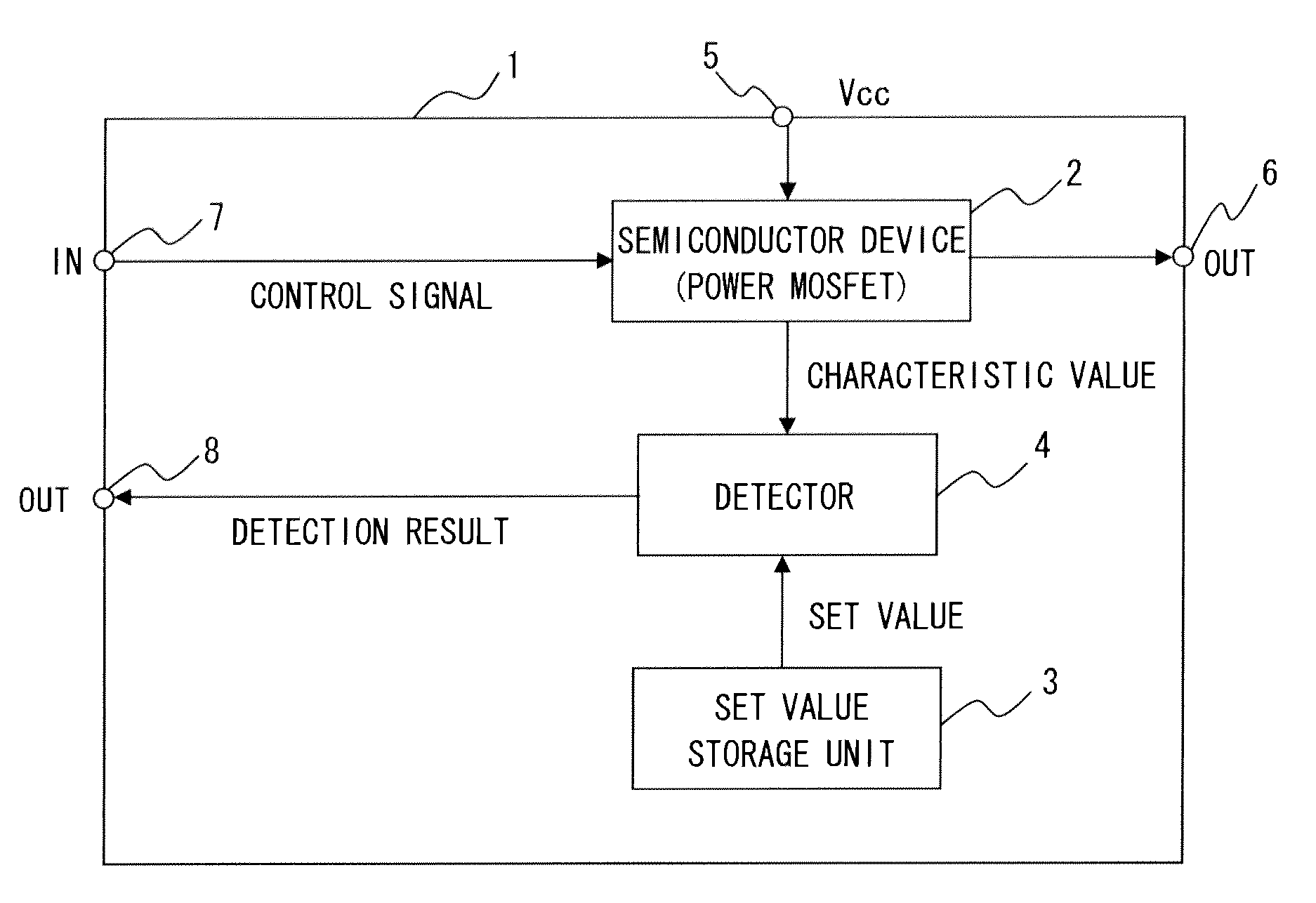
[0072]A first exemplary embodiment of the present invention is described hereinafter with reference to the drawings. FIG. 1 is a block diagram showing an IPD (semiconductor apparatus) 1 according to the exemplary embodiment. The IPD 1 according to the exemplary embodiment is manufactured by a semiconductor manufacturing process, and the IPD 1 includes a set value storage unit 3 that stores a set value which is determined based on an initial characteristic value of the IPD 1 in the state where a semiconductor chip (or wafer) is completed, and a detector 4 that detects the characteristic degradation of the IPD 1 based on a characteristic value of the IPD 1 at given timing in the state where the IPD 1 is implemented in a system such as an engine control unit (ECU) and the set value stored in the set value storage unit 3.

[0073]A power semiconductor device which is included in the IPD 1 according to the exemplary embodiment is a power MOSFET 2, for example. The power MOSFET 2 is an N-typ...

second exemplary embodiment

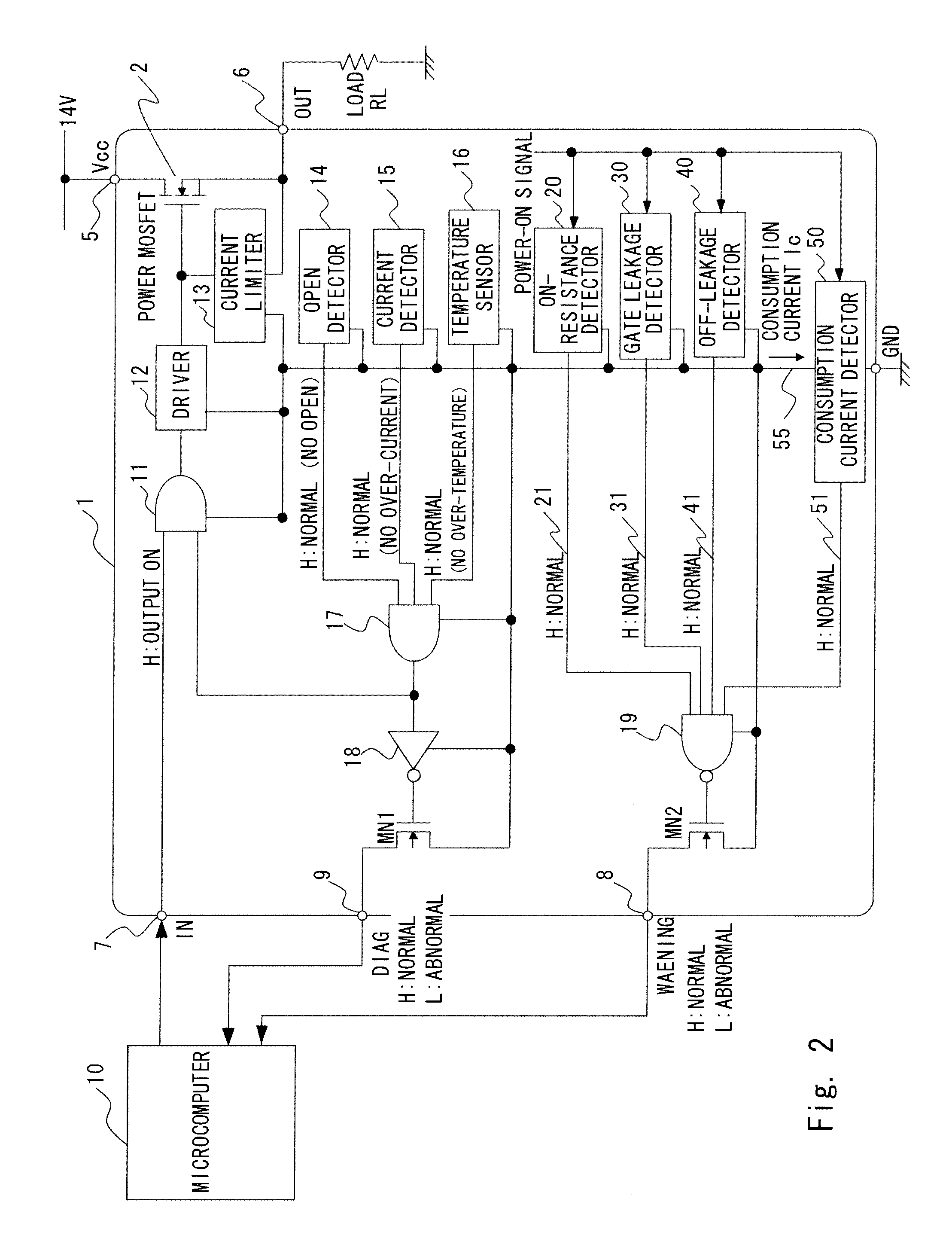
[0138]A second exemplary embodiment of the present invention is described hereinafter with reference to the drawings. FIG. 9 is a block diagram showing an IPD (semiconductor apparatus) according to the exemplary embodiment. In the IPD 1a according to the exemplary embodiment, the outputs of the on-resistance detector 20, the gate leakage detector 30, the off-leakage detector 40, and the consumption current detector 50 are output also to an AND circuit 70, and the output of the AND circuit 70 is supplied to the AND circuit 11. The other part is the same as that of the IPD 1 described in the first exemplary embodiment, and redundant explanation thereof is omitted. Note that the same elements as in the IPD 1 described in the first exemplary embodiment are denoted by the reference symbols. Further, although connections between the line at the L level of the respective elements that constitute the IPD 1a and the consumption current detector 50 are not illustrated in FIG. 9 to avoid compl...


PUM


Abstract

A semiconductor apparatus (IPD) includes a set value storage unit that stores a set value determined based on an initial characteristic value of the IPD, and a detector that detects characteristic degradation of the IPD based on a characteristic value of the IPD at given timing and the set value stored in the set value storage unit. Further, a method of detecting characteristic degradation of a semiconductor apparatus (IPD) includes storing a set value determined based on an initial characteristic value of the IPD, and detecting characteristic degradation of the IPD based on a characteristic value of the IPD at given timing and the stored set value.

Description

INCORPORATION BY REFERENCE[0001]This application is based upon and claims the benefit of priority from Japanese patent application No. 2009-218824, filed on Sep. 24, 2009, the disclosure of which is incorporated herein in its entirety by reference.BACKGROUND[0002]1. Field of the Invention[0003]The present invention relates to a semiconductor apparatus and a method of detecting characteristic degradation of a semiconductor apparatus and, particularly, to a semiconductor apparatus and a method of detecting characteristic degradation of a semiconductor apparatus that detect characteristic degradation of a semiconductor apparatus which is a so-called intelligent power device (IPD).[0004]2. Description of Related Art[0005]A power MOSFET is one of devices capable of handling a large power. The power MOSFET has a feature such as a higher switching speed than other power devices.[0006]Japanese Unexamined Patent Application Publication No. 2007-174756 discloses an on-failure detection appara...

Claims


Application Information

Patent Timeline
Patent Type & Authority Applications(United States)
IPC IPC(8): G01R31/26
CPCG01R31/2642
Inventor FUKAMI, IKUO
Owner RENESAS ELECTRONICS CORP
Why Eureka
Try Eureka