NAND flash memory
- Summary
- Abstract
- Description
- Claims
- Application Information
AI Technical Summary
Problems solved by technology
Method used
Image

Examples
first embodiment
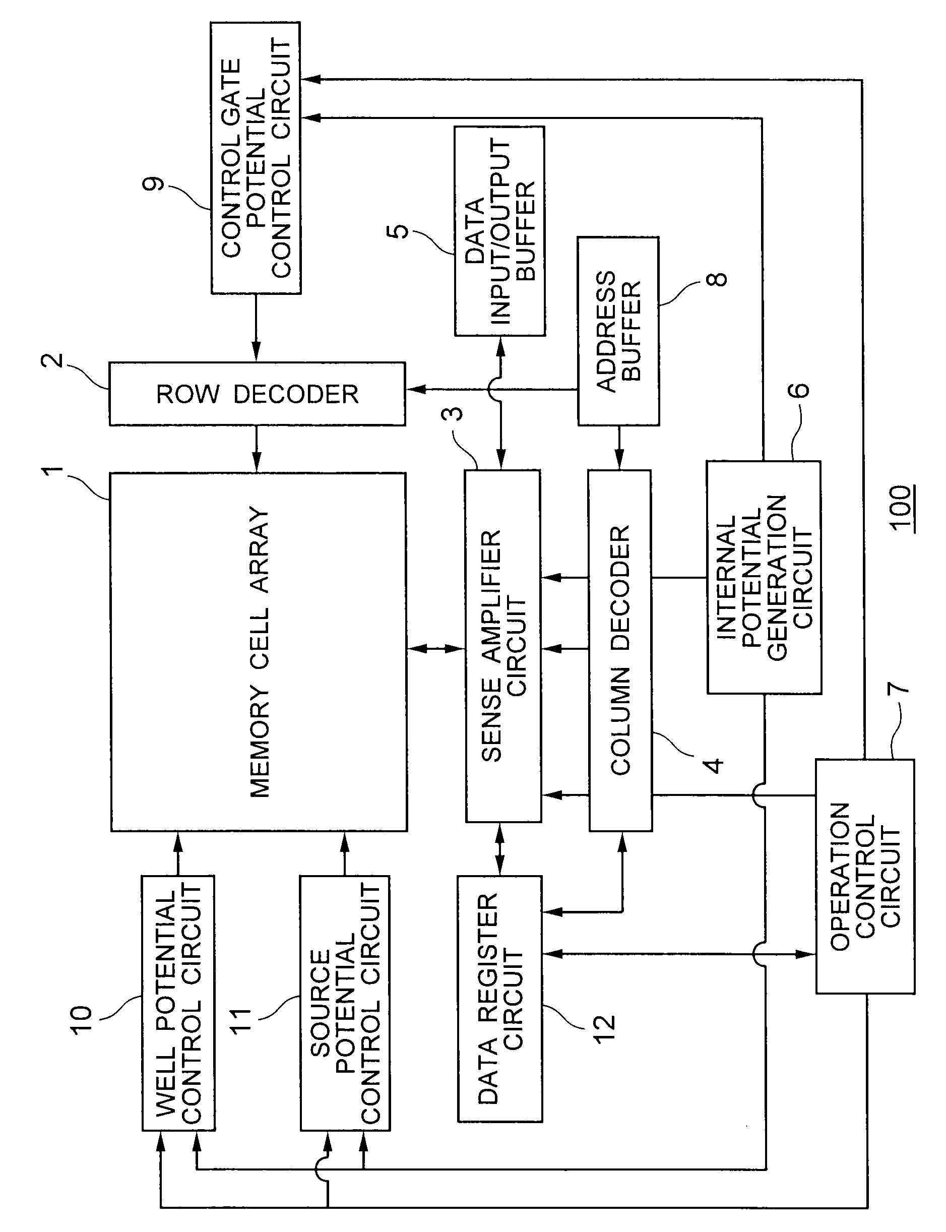
[0049]FIG. 5 is a block diagram showing a configuration of a principal part of a NAND flash memory 100 according to a first embodiment.
[0050]As shown in FIG. 5, the NAND flash memory 100 includes a memory cell array 1, a row decoder 2, a sense amplifier circuit 3, a column decoder 4, a data input / output buffer 5, an internal potential generation circuit 6, an operation control circuit 7, an address buffer 8, a control gate potential control circuit 9, a well potential control circuit 10, a source potential control circuit 11, and a data register circuit 12.
[0051]The memory cell array 1 includes a plurality of NAND strings arranged in a matrix form and connected to word lines WL in the row direction and bit lines BL in the column direction as described below.
[0052]The row decoder 2 includes a word line drive circuit (not illustrated), and conducts word line selection and drive of the memory cell array 1.
[0053]The sense amplifier circuit 3 includes a circuit (not illustrated) which co...
second embodiment
[0116]In the first embodiment, the case where data stored in the memory cell transistor is a binary value (1 bit) has been described.
[0117]In embodiments according to the present invention, application to the case where data assumes a multiple value is also possible.
[0118]In the present second embodiment, therefore, the case where data stored in the memory cell transistor assumes a multiple value (especially four values (2 bits)) will be described.
[0119]In the same way as the first embodiment, a method described in the second embodiment is executed by, for example, the NAND flash memory 100 shown in FIG. 5. Read operation of the NAND flash memory 100 is the same as that in the first embodiment.
[0120]The second embodiment differs in the configuration of the data register circuit 12 from the first embodiment. FIG. 12 is a diagram showing another example of configurations of the sense amplifier circuit 3 and the data register circuit 12.
[0121]As shown in FIG. 12, the sense amplifier ci...
third embodiment
[0164]In the second embodiment, an example of the case where data stored in the memory cell transistor assumes a multiple value has been described.
[0165]In the present third embodiment, another example of the case where data stored in the memory cell transistor assumes a multiple value (especially four value (2 bits)) will be described.
[0166]In the same way as the second embodiment, a method described in the present third embodiment is executed by, for example, the NAND flash memory 100 shown in FIG. 5. Read operation of the NAND flash memory 100 is the same as that in the first embodiment.
[0167]The third embodiment is the same in the configuration of the data register circuit 12 as the second embodiment.
[0168]In the present third embodiment as well, the already described stepup write scheme is used. Write operation of data of low order (a first bit) of the NAND flash memory 100 according to the third embodiment is the same as that in the second embodiment (FIG. 13). Relations among...
PUM
 Abstract
Description
Claims
Application Information
 - R&D Engineer
- R&D Manager
- IP Professional
- Industry Leading Data Capabilities
- Powerful AI technology
- Patent DNA Extraction
Browse by: Latest US Patents, China's latest patents, Technical Efficacy Thesaurus, Application Domain, Technology Topic.
© 2024 PatSnap. All rights reserved.Legal|Privacy policy|Modern Slavery Act Transparency Statement|Sitemap