Automatic Positioning of Gate Array Circuits in an Integrated Circuit Design

a gate array circuit and integrated circuit technology, applied in the field of integrated circuit design, can solve the problems of complex and expensive production of each such mask used in the integrated circuit manufacturing process, functional problems or circuit timing problems of logic cells, and possible gaps or empty spaces between certain adjacent logic cells

Active Publication Date: 2011-03-24
GLOBALFOUNDRIES US INC
View PDF21 Cites 117 Cited by
  • Summary
  • Abstract
  • Description
  • Claims
  • Application Information

AI Technical Summary

Problems solved by technology

After the logic cells are positioned in the integrated circuit chip design, gaps or empty spaces are likely to remain between certain adjacent logic cells.
Each such mask used in an integrated circuit manufacturing process is very complicated and expensive to produce.
A problem with an integrated circuit design, such as a functional problem or a circuit timing problem with a logic cell, may be discovered after integrated circuit manufacturing processes, such as mask fabrication or even semiconductor processing, have been begun, or even have been completed.
The requirement for a design change late in the integrated circuit fabrication process is almost unavoidable, due to the complexity of integrated circuit designs in combination with increasingly tight time-to-market requirements for new designs.
A design change to the logic cells at this point might require scrapping masks or even processed semiconductor substrates and could be very expensive.
A particular challenge is to maximize the gate array fill circuits that remain available for configuration even as other gate array fill circuits are configured into gate array logic elements to implement needed circuit design changes.
Maximizing gate array fill circuit density in an efficient manner is constrained by the limitations of current integrated circuit manufacturing processes and limited by currently available methods for positioning of configurable gate array fill circuits and fully configured gate array logic elements in an integrated circuit design.
Of course, such a manual approach is time consuming.

Method used


Image

  • Automatic Positioning of Gate Array Circuits in an Integrated Circuit Design
  • Automatic Positioning of Gate Array Circuits in an Integrated Circuit Design
  • Automatic Positioning of Gate Array Circuits in an Integrated Circuit Design

Examples


Embodiment Construction

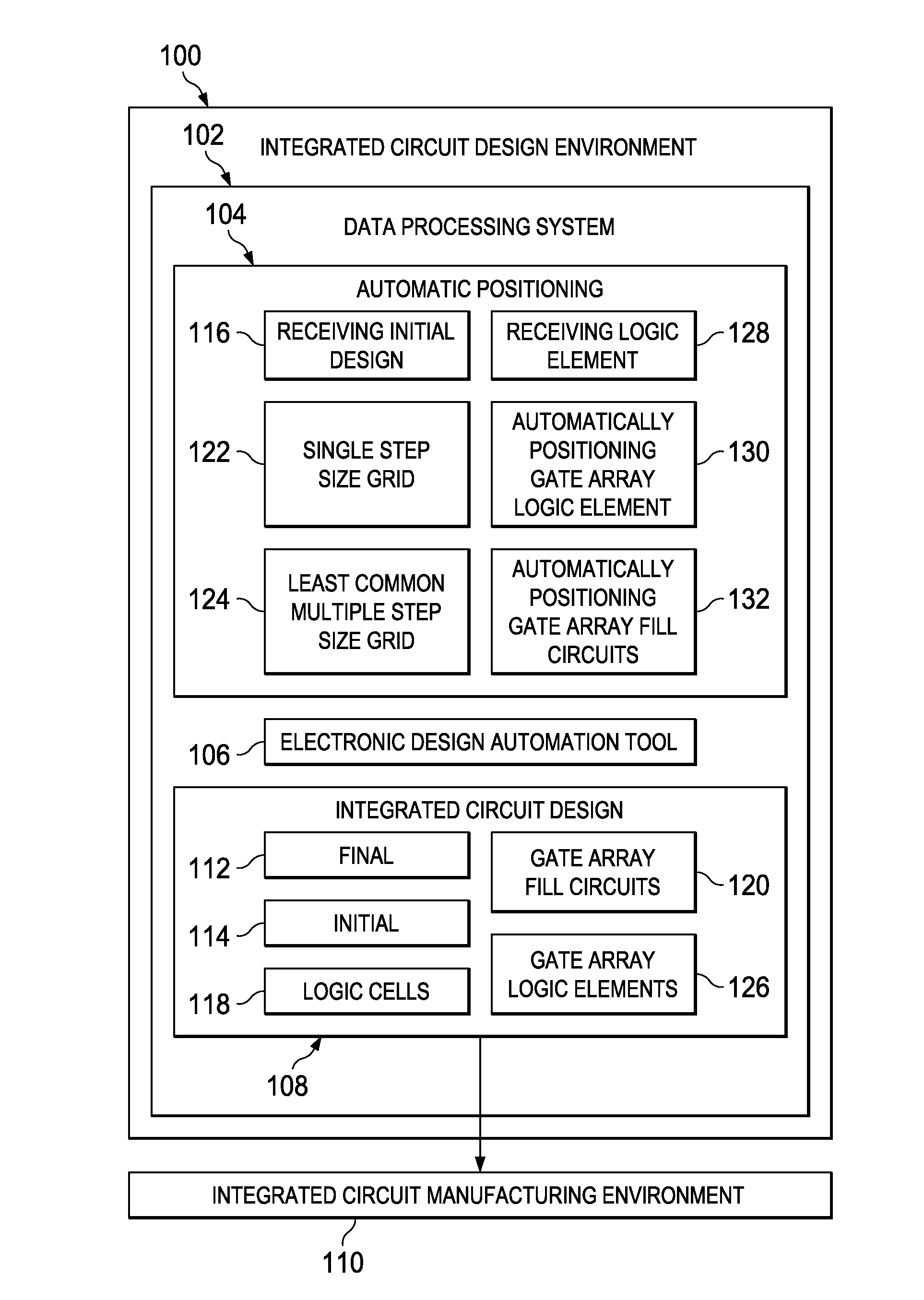
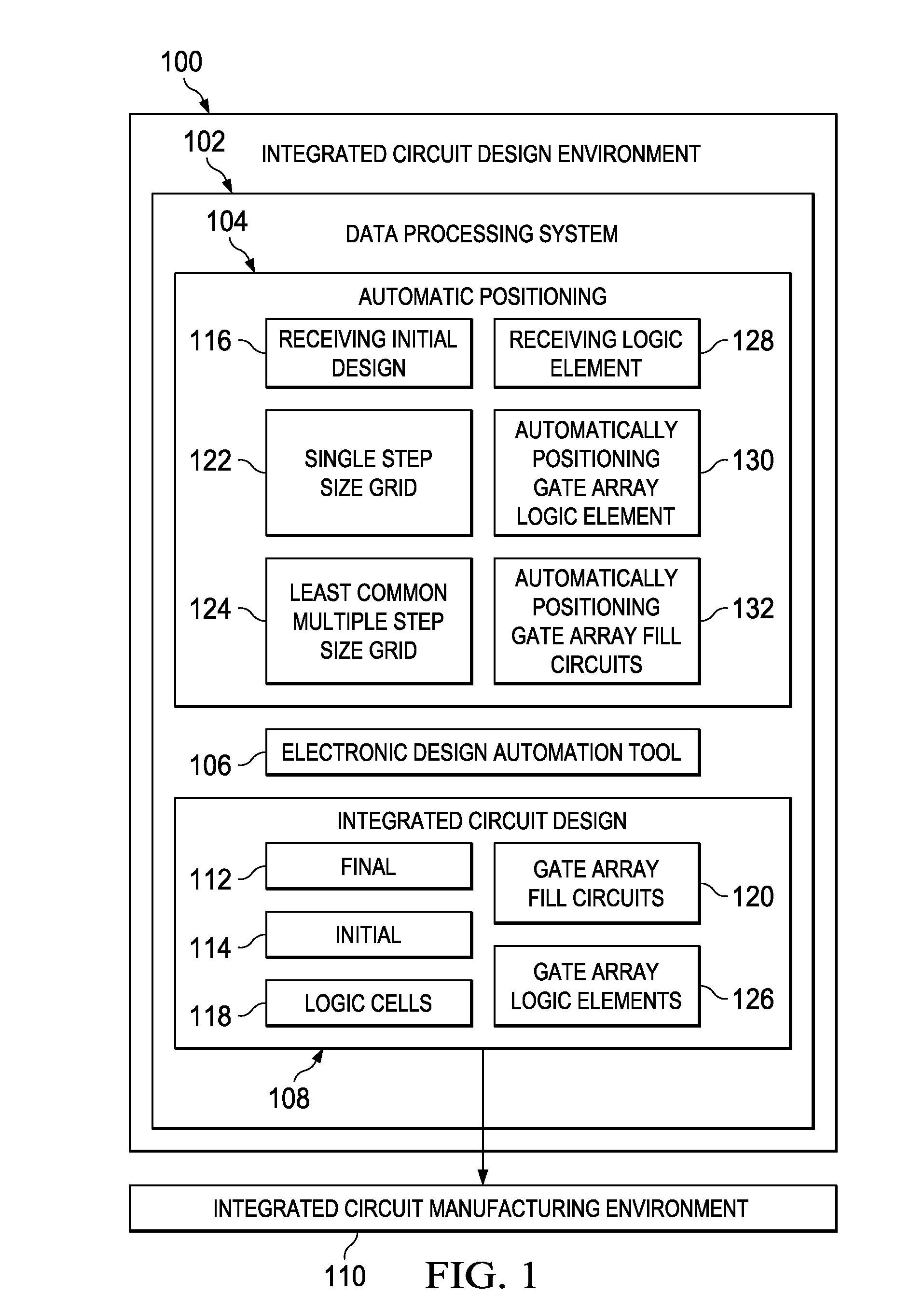
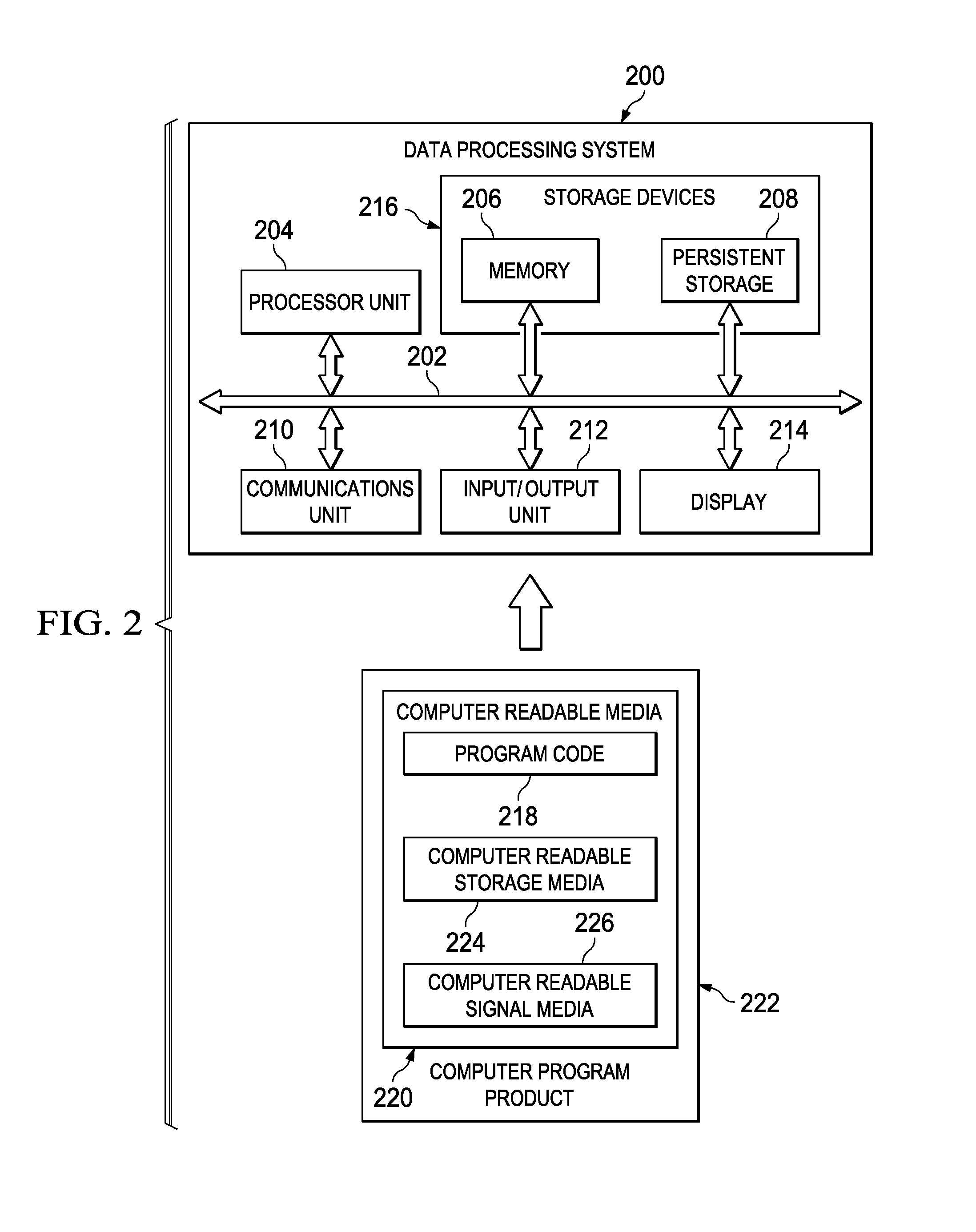
[0031]A method and apparatus by which arbitrarily positioned gate array fill circuits may be automatically replaced with fully configured gate array logic elements in an integrated circuit design process is disclosed. An illustrative integrated circuit design environment 100, in which an illustrative method and apparatus for the positioning of gate array logic elements and gate array fill circuits in an integrated circuit design may be implemented, is presented in summary in the functional block diagram of FIG. 1. Integrated circuit design environment 100 may include data processing system 102 upon which an illustrative method for the positioning of gate array logic elements and gate array fill circuits in an integrated circuit design may be implemented. As will be discussed in more detail below, data processing system 102 may include one or more general purpose or specialized computers or computer systems or other data processing systems that are operated to implement the functiona...


PUM


Abstract

An automated method and apparatus for positioning gate array circuits in an integrated circuit design. An initial integrated circuit design includes logic cells and gate array fill circuits positioned thereon. The gate array fill circuits are positioned in available space between the adjacent logic cells so as to fill the available space with the maximum gate array fill circuits. A gate array logic element to be positioned in the integrated circuit design, such as may be required by an engineering change to the circuit design, is automatically positioned between adjacent logic cells so as to allow for full utilization of any space remaining between the adjacent logic cells by gate array fill circuits.

Description

BACKGROUND[0001]1. Field[0002]This disclosure relates generally to integrated circuit design, and more specifically to the placement of gate array circuits in an integrated circuit design.[0003]2. Description of the Related Art[0004]Logic synthesis is a computer implemented process that transforms a circuit description from one level of abstraction to a lower level, usually towards the physical implementation of an integrated circuit. As a result of the logic synthesis process, logic cells or logic functions are arranged physically on an integrated circuit chip in multiple circuit rows and / or circuit columns in order to form the completed design. Each circuit row and / or circuit column on the integrated circuit chip contains multiple logic cells that are arranged adjacent to one another.[0005]After the logic cells are positioned in the integrated circuit chip design, gaps or empty spaces are likely to remain between certain adjacent logic cells. These empty spaces, sometimes referred...

Claims


Application Information

Patent Timeline
Patent Type & Authority Applications(United States)
IPC IPC(8): G06F17/50
CPCG06F17/5072G06F30/392
Inventor KEINERT, JOACHIMLAMB, DOUGLASS T.LEWIS, DAVID W.RAMJI, SHYAM
Owner GLOBALFOUNDRIES US INC
Why Eureka
Try Eureka