Non-contact interface system

a technology of contact interface and interface system, which is applied in the direction of inductance, testing/measurement of semiconductor/solid-state devices, transportation and packaging, etc., can solve the problems of reducing the resistance associated with the size of the coil, exposing the sensor wafer to harsh conditions, and high levels of electromagnetic and other radiative nois

Inactive Publication Date: 2011-03-31
KLA TENCOR TECH CORP
View PDF12 Cites 32 Cited by
  • Summary
  • Abstract
  • Description
  • Claims
  • Application Information

AI Technical Summary

Problems solved by technology

During the measurement process, these sensor wafers may be exposed to harsh conditions such as excessive heat, corrosive chemicals, and bombardment by high energy ions, and high levels of electromagnetic and other radiative noise.
The current trend amongst wafer sensors and FOUPs is to scale down the size of primary and secondary coils, thus reducing the resistance associated with the size of the coil.
Particle generation affects the accuracy of the survey process and creates a barrier for entry into particle sensitive applications.

Method used


Image

  • Non-contact interface system
  • Non-contact interface system
  • Non-contact interface system

Examples


Embodiment Construction

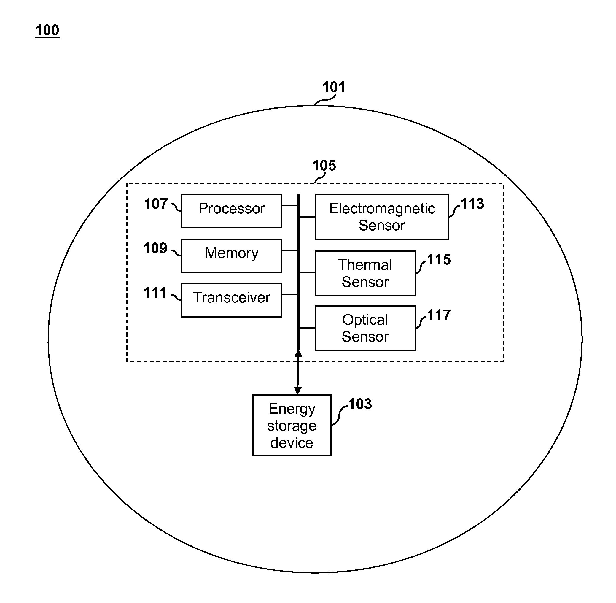
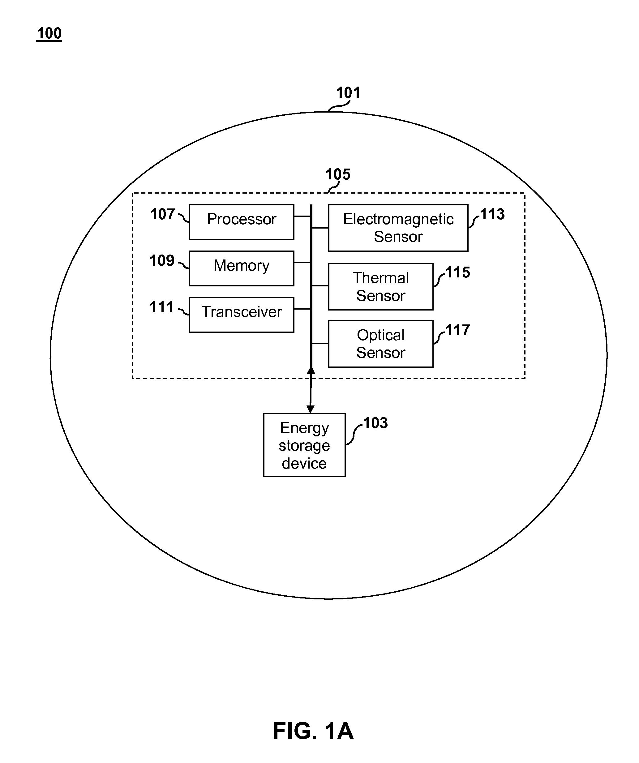
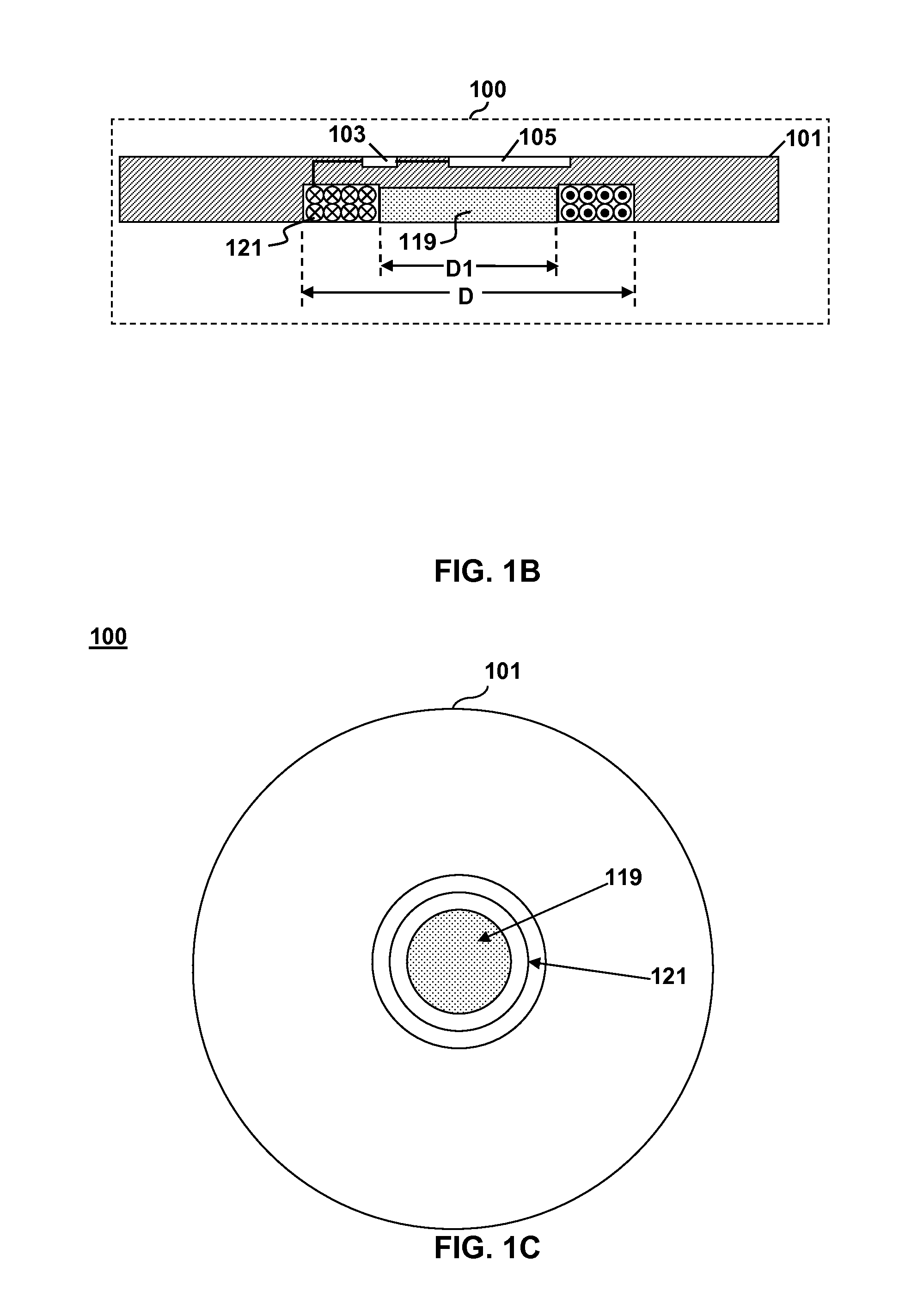
[0013]Embodiments of the present invention overcome the disadvantages associated with the prior art by increasing the diameters of the primary and secondary coils used to charge and / or communicate with a sensor wafer. As a result of the increased coil size, a large inter-coil spacing may be used.

[0014]FIGS. 1A-1C illustrate an example of a sensor wafer 100 configured to measure process parameters in a system for processing wafers during semiconductor fabrication. The sensor wafer 100 may include a substrate 101, with an energy storage device 103 and measurement electronics 105 mounted to the substrate 101. By way of example, and not by way of limitation, the measurement electronics 105 of the sensor wafer 100 may be implemented with a processor module 107, a main memory 109, a transceiver 111, and one or more sensors 113, 115, 117. The substrate 101 may have the same dimensions as a production substrate that is processed by a semiconductor device fabrication system, e.g., 150 mm, 20...


PUM


Abstract

An interface system for a sensor wafer may comprise a sensor wafer having a substrate. One or more sensors may be mounted to the substrate. An electronics module may be mounted to the substrate and coupled to the one or more sensors. An energy storage device may be mounted to the substrate and coupled to the electronics module. A secondary coil may be attached to a surface of the sensor wafer, and coupled to the electronics module of the sensor wafer, having a diameter of at least 50 millimeters. A primary coil may be attached to a front opening universal pod (FOUP). The primary coil, may situated and oriented in the FOUP such that the primary coil is concentric with the secondary coil and at least 8, but less than 12 millimeters from the sensor wafer when the sensor wafer is stored in a slot in the FOUP.

Description

BACKGROUND OF INVENTION[0001]Sensor wafers are used to obtain non-invasive, in-situ measurements of actual physical and electrical properties of plasma within an operational plasma processing environment. These sensor wafers are configured to collect, process, and store data received during measurement of the plasma. These sensor wafers may include devices to measure thermal, optical, and electromagnetic properties of the process environment. During the measurement process, these sensor wafers may be exposed to harsh conditions such as excessive heat, corrosive chemicals, and bombardment by high energy ions, and high levels of electromagnetic and other radiative noise. It is important for the sensor wafer to remain resilient in the harsh environment associated with in-situ measurement of plasma.[0002]Sensor wafers are currently housed and stored in a front operating universal pod (FOUP) during the in-situ process survey. A FOUP is a specialized plastic enclosure designed to hold waf...

Claims


Application Information

Patent Timeline
Patent Type & Authority Applications(United States)
IPC IPC(8): H02J17/00H02J7/00
CPCH02J7/025H01L21/67253H04B5/0043H02J7/0044H02J50/005H02J50/10H01L22/00H01L21/673
Inventor JENSEN, EARLMASON, ARON
Owner KLA TENCOR TECH CORP
Why Eureka
Try Eureka