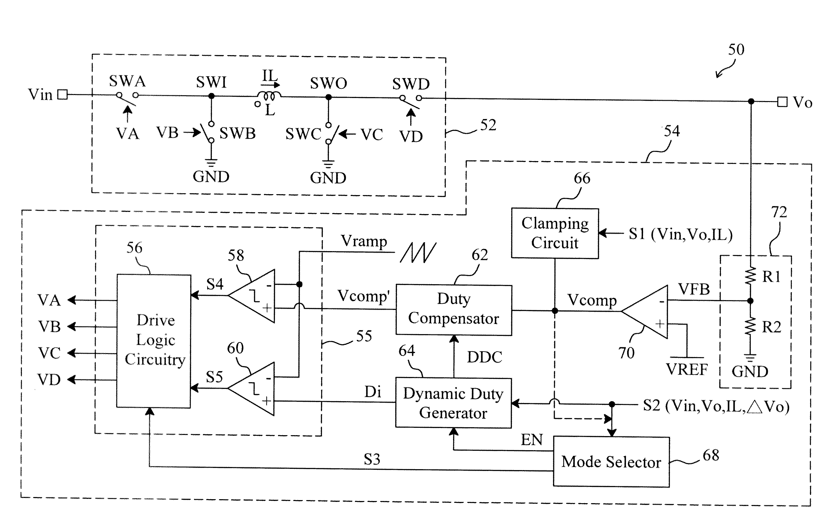
[0030]In an embodiment according to the present invention, as shown in FIG. 3, a buck-boost power converter 50 includes a buck-boost power stage 52 and a control circuit 54 to provide control signals VA, VB, VC and VD to switch the power switches SWA, SWB, SWC and SWD connected to an inductor L in the buck-boost power stage 52 to convert an input voltage Vin to an output voltage Vo. In the control circuit 54, a feedback circuit 72 detects the output voltage Vo to generate a feedback signal VFB, an error amplifier 70 amplifies the difference between the feedback signal VFB and a reference voltage VREF to generate an error signal Vcomp, a clamping circuit 66 clamps the level of the error signal Vcomp according to a detecting signal S1 related to at least one of the input voltage Vin, output voltage Vo and inductor current IL, a mode selector 68 generates a mode switch signal S3 according to a detecting signal S2 related to at least one of the input voltage Vin, output voltage Vo, inductor current IL and variation ΔVo of the output voltage Vo for a drive logic circuitry 56 and an enable signal EN to enable a dynamic duty generator 64, the dynamic duty generator 64 determines a dynamic duty insertion signal Di and a compensation signal DDC according to the detecting signal S2, a duty compensator 62 compensates the error signal Vcomp to generate a compensated error signal Vcomp′ according to the compensation signal DDC, and a driver 55 generates the control signals VA, VB, VC and VD according to a ramp signal Vramp, the compensated error signal Vcomp′, the duty insertion signal Di and the mode switch signal S3. Alternatively, in other embodiments, the mode selector 68 may generate the signals S3 and EN according to the error signal Vcomp, instead of the detecting signal S2. The driver 55 includes a comparator 58 to compare the compensated error signal Vcomp′ with the ramp signal Vramp to generate a comparison signal S4, a comparator 60 to compare the ramp signal Vramp with the duty insertion signal Di to generate a comparison signal S5, and the drive logic circuitry 56 to determine the control signals VA, VB, VC and VD according to the signals S3, S4 and S5.
[0031]FIG. 4 shows the current paths of the buck-boost power stage 52 in a buck mode, in which mode the power switch SWC keeps off and the power switch SWD keeps on. A buck charge path 74 is established if the power switch SWA is on and the power switch SWB is off, and a buck discharge path 76 is established if the power switch SWA is off and the power switch SWB is on. FIG. 5 shows the current paths of the buck-boost power stage 52 in a buck-boost mode, in which mode a boost charge path 78 is established if the power switches SWA and SWC are on and the power switches SWB and SWD are off, a buck charge path or boost discharge path 80 is established if the power switches SWA and SWD are on and the power switches SWB and SWC are off, and a buck discharge path 82 is established if the power switches SWB and SWD are on and the power switches SWA and SWC are off. FIG. 6 shows the current paths of the buck-boost power stage 52 in a boost mode, in which mode the power switch SWA keeps on and the power switch SWB keeps off. A boost charge path 86 is established if the power switch SWC is on and the power switch SWD is off, and a boost discharge path 84 is established if the power switch SWC is off and the power switch SWD is on.
[0032]FIG. 7 is a waveform diagram of the buck-boost power converter 50 from a buck mode to a buck-boost mode, in which waveform 90 represents the compensated error signal Vcomp′, waveform 92 represents the ramp signal Vramp, waveform 94 represents the duty insertion signal Di, and waveform 96 represents the inductor current IL. Referring to FIGS. 3 and 7, in the buck mode, the dynamic duty generator 64 is turned off, so the duty insertion signal Di is zero. As a result, the power switch SWC keeps off and the power switch SWD keeps on. In this case, the compensated error signal Vcomp′ and the ramp signal Vramp control the power switches SWA and SWB to control the inductor current IL to increase or decrease, as shown by the waveforms 90, 92 and 96. During a buck charge period D2′, e.g., from time t6 to time t7, the power switch SWA is on and the power switch SWB is off, so the inductor current IL increases. During a buck discharge period D3′, e.g., from time t7 to time t8, the power switch SWA is off and the power switch SWB is on, so the inductor current IL decreases. When entering the buck-boost mode from the buck mode, e.g., at time t8, the mode selector 68 asserts the enable signal EN to enable the dynamic duty generator 64, so the duty insertion signal Di becomes non-zero, as shown by the waveform 94, and thus a boost charge period D1 results, e.g., from time t8 to time t9. Because the duty insertion signal Di varies with the detecting signal S2, the boost charge period D1 also varies with the detecting signal S2. To avoid large output ripple resulted from the inserted boost charge period D1, the dynamic duty generator 64 may send out the compensation signal DDC to the duty compensator 62 so that the compensated error signal Vcomp′ decreases as the duty insertion signal Di increases, as shown by the waveforms 90 and 94. Thereby, the buck charge period decreases from D2′ to D2, and the buck discharge period increases from D3′ to D3. Thus, as shown at time t8 and time t11, the initial level and the ending level of the inductor current IL are the same in each cycle, so large output ripple can be avoided. As can be seen from the waveform 96 of FIG. 7, the duration from time t8 to time t11 is a cycle, in which a boost charging state is from time t8 to time t9, a buck charging state is from time t9 to time t10, and a buck discharging state is from time t10 to time t11. No duplicated state appears in each cycle; in other words, the switching sequence of the power switches SWA, SWB, SWC and SWD is optimized by the control circuit 54 of the present invention, so the switching loss is minimized. In this embodiment, although only the operation of switching from a buck mode to a buck-boost mode is described, the operation of switching from a boost mode to a buck-boost mode will be readily known by those skilled in the art and, thus, will not be further described herein.
[0033]FIG. 8 is a waveform diagram of the buck-boost power converter 50 from a power saving mode to normal operation, in which waveform 100 represents the compensated error signal Vcomp′, waveform 102 represents the ramp signal Vramp, waveform 104 represents the duty insertion signal Di, and waveform 106 represents the inductor current IL. To save energy, power converters currently available are all set to have a power saving mode, for example a pulse skipping mode (PSM). When a conventional buck-boost power converter needs to switch back to a buck-boost mode from a power saving mode, it must first enter a buck mode and then, after the error signal Vcomp increases to a threshold value from zero, enters a buck-boost mode. However, it may take several cycles for the error signal Vcomp to increase to the threshold value from zero. Referring to FIG. 8, when the buck-boost power converter 50 of the present invention switches back to a buck-boost mode from a power saving mode, it switches back to a buck mode from the power saving mode in a first cycle. Because the clamping circuit 66 can dynamically clamp the level of the error signal Vcomp according to the detecting signal S1, it is unnecessary for the error signal Vcomp to increase slowly from zero. Moreover, the dynamic duty generator 64 is turned off in the buck mode, so Vcomp′=Vcomp. In other words, the compensated error signal Vcomp′ is clamped at a level close to the threshold value, as shown by the waveform 100. Thereby, the buck-boost power converter 50 enters the buck-boost mode from the buck mode immediately in a second cycle, and terminates the transient response in a third cycle. In other words, the clamping circuit 66 in the control circuit 54 can speed up the transient response that is switching from the power saving mode back to the buck-boost mode.
[0034]FIG. 9 is a waveform diagram of the buck-boost power converter 50 in a buck-boost mode, in which waveform 110 represents the compensated error signal Vcomp′, waveform 112 represents the ramp signal Vramp, waveform 114 represents the duty insertion signal Di, waveform 116 represents the inductor current IL, and waveform 118 represents the average value of the inductor current IL. In the buck-boost mode, when the duty insertion signal Di increases, as shown by the waveform 114, the boost charge period D1 increases. Thereby, the average value of the inductor current IL increases correspondingly, as shown by the waveform 118, and meanwhile, the dynamic duty generator 64 outputs the compensation signal DDC to the duty compensator 62 to decrease the compensated error signal Vcomp′, as shown by the waveform 110. When the duty insertion signal Di changes, the average value of the inductor current IL also changes correspondingly, so it is unnecessary for the control circuit 54 to adjust the inductor current IL according to the error signal Vcomp.
[0035]FIG. 10 is a circuit diagram of an embodiment for the duty compensator 62 shown in FIG. 3. The error signal Vcomp from the error amplifier 70 is transmitted to a voltage dividing circuit 122 and a resistor R3 through buffers 120 and 124, respectively. The voltage dividing circuit 122 consisting of a plurality of resistors RD1-RDN and a plurality of switches SW1-SWN divides the error signal Vcomp to generate a divided error voltage Vd, and the switches SW1-SWN are controlled by the compensation signal DDC from the dynamic duty generator 64. A voltage-to-current converter 126 converts the divided error voltage Vd into a compensating current Id, which flows through the resistor R3 to generate a compensating voltage VR3, and the compensated error signal Vcomp′ is obtained by subtracting the compensating voltage VR3 from the error signal Vcomp.
[0036]FIG. 11 is a circuit diagram of an embodiment for the drive logic circuitry 56, dynamic duty generator 64 and mode selector 68 shown in FIG. 3. In FIG. 11, a ramp generator 130 consisting of a switch M2, a current source Ich and a capacitor C provides the ramp signal Vramp. The drive logic circuitry 56 includes inverters 140 and 144 and a NAND gate 142, in which the signal S4 from the comparator 58 functions as the control signal VB, the inverter 140 inverts the control signal VB to generate the control signal VA, the NAND gate 142 generates the control signal VD according to the signals S3 and S5, and the inverter 144 inverts the control signal VD to generate the control signal VC. In the dynamic duty generator 64, an analog-to-digital converter 132 converts the detecting signal S2 into the compensation signal DDC, which is a digital signal, and then a digital-to-analog converter 134 converts the compensation signal DDC into the duty insertion signal Di, which is an analog signal. The mode selector 68 includes a comparator 138 to compare the detecting signal S2 with a threshold value VTH to generate the mode switch signal S3. The threshold value VTH is used to determine whether to switch the power converter 50 to the buck-boost mode, which may be a fixed value, or be dependent on the inductor current IL or the variation of the output voltage Vo. A dynamic threshold value VTH can help to improve the efficiency of the power converter 50 and the ripple of the output voltage Vo, and additionally, accelerate the transient response of a load or a power source. In the case that the threshold value VTH varies with the inductor current IL, when the load is heavier and the inductor current is larger, the threshold value VTH is increased to have the buck-boost power converter 50 work in the buck-boost mode, in which mode the charge or discharge process is accelerated to prevent occurrence of undue ripple. In the case that the threshold value VTH varies with the variation of the output voltage Vo, when the variation of the output voltage Vo increases, the threshold value VTH increases to enlarge the operating area to enter the buck-boost mode, in which mode the inductor current IL is easy to be charged or discharged, thereby reducing the ripples of the output voltage Vo.
[0037]In other embodiments, a fixed duty generator that provides a fixed signal may be used to replace the dynamic duty generator 64.
[0038]While the present invention has been described in conjunction with preferred embodiments thereof, it is evident that many alternatives, modifications and variations will be apparent to those skilled in the art. Accordingly, it is intended to embrace all such alternatives, modifications and variations that fall within the spirit and scope thereof as set forth in the appended claims.