Unlock instant, AI-driven research and patent intelligence for your innovation.

Block management method for a flash memory and flash memory controller and storage system using the same

a management method and flash memory technology, applied in the direction of memory adressing/allocation/relocation, instruments, computing, etc., can solve the problems of physical blocks being damaged, limited number of times of erasing physical blocks of physical units, etc., to achieve the effect of prolonging the lifespan of flash memory storage devices

Active Publication Date: 2011-03-31
SAMSUNG ELECTRONICS CO LTD
View PDF3 Cites 51 Cited by
  • Summary
  • Abstract
  • Description
  • Claims
  • Application Information

AI Technical Summary

Benefits of technology

[0009]The present invention is directed to a block management method capable of effectively prolong the lifespan of a flash memory storage device.
[0010]The present invention is directed to a flash memory controller capable of effectively prolong the lifespan of a flash memory storage device.
[0011]The present invention is directed to a flash memory storage system capable of effectively prolong the lifespan of a flash memory storage device.
[0016]As described above, the block management method can effectively prolong the lifespan of a flash memory storage device.

Problems solved by technology

Therefore, under a normal access mode, the host system can not access the physical blocks in the system area and the replacement area.
However, the number of times of erasing the physical blocks of physical units is limited (for instance, the physical blocks will be damaged after ten thousand times of erasing).
In particular, when damaged physical blocks exceed a certain amount with a result that the number of physical blocks becomes insufficient for access of the host system, the flash memory storage device would enter a write protect status or be determined as useless.
And, the block management method further includes obtaining a deleted logical block and marking each of the logical addresses mapped to the deleted logical block as a bad logical address, wherein data stored in the logical addresses mapped to the deleted logical block is recognized as invalid by the host system and the host system is not allowed to access data in the bad logical address.

Method used


Image

  • Block management method for a flash memory and flash memory controller and storage system using the same
  • Block management method for a flash memory and flash memory controller and storage system using the same
  • Block management method for a flash memory and flash memory controller and storage system using the same

Examples


first exemplary embodiment

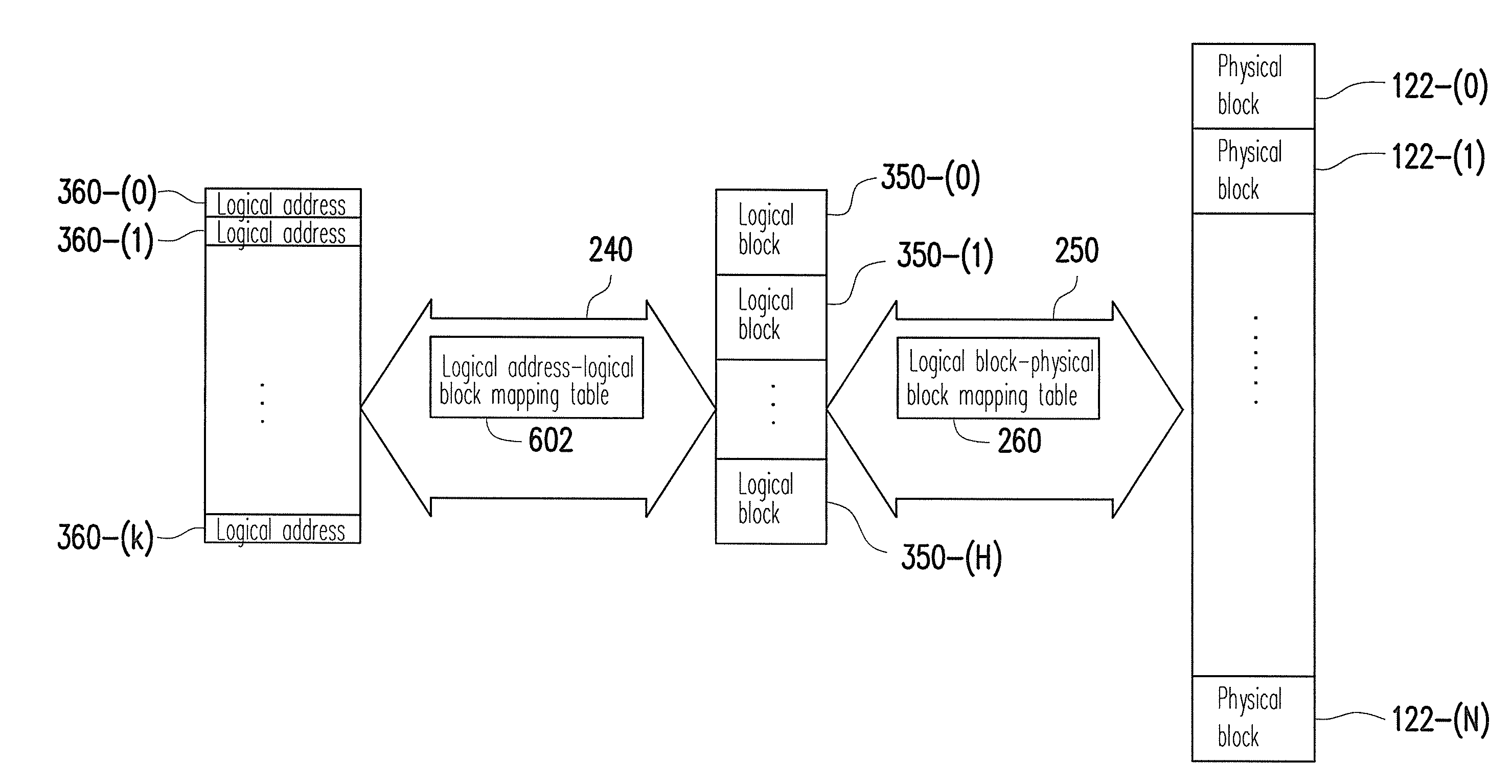
[0034]FIG. 1A is a schematic block diagram of a host system and a flash memory storage device according to a first exemplary embodiment of the present invention.

[0035]Referring to FIG. 1A, a host system 1000 includes a computer 1100 and an input / output (I / O) device 1106. The computer 1100 includes a microprocessor 1102, a random access memory (RAM) 1104, a system bus 1108, and a data transmission interface 1110. For example, the I / O device 1106 includes a mouse 1202, a keyboard 1204, a display 1206 and a printer 1208 as shown in FIG. 1B. It should be understood that the devices illustrated in FIG. 1B are not intended to limiting the I / O device 1106, and the I / O device 1106 may further include other devices.

[0036]In the present embodiment, the flash memory storage device 100 is coupled to other devices of the host system 1000 through the data transmission interface 1110. The host system 1000 writes data into or reads data from the flash memory storage device 100 through the operation...

second exemplary embodiment

[0074]A flash memory storage device and a host system in the second exemplary embodiment essentially are similar to the flash memory storage device and the host system in the first exemplary embodiment, wherein the difference is a memory management unit in the second exemplary embodiment re-maps the logical addresses to the logical blocks to concentrate several deleted logical addresses into the same logical block. Here, FIGS. 1A, 1D and 3A are used for describing the second exemplary embodiment of the present invention.

[0075]In the first exemplary embodiment, when all the physical blocks in the spare area 306 become bad physical blocks or can not be used normally, and there is no any normal physical block in the replacement area 308, the flash memory controller 104 finds a delete logical block based on the deleting records. That is, the memory management unit 204 finds the deleted logical block among the logical blocks, wherein all the data stored in the logical addresses belonging...


PUM


Abstract

A block management method for managing a plurality of physical blocks of a flash memory chip is provided. The block management method includes configuring a plurality of logical addresses; mapping the logical addresses to a plurality of logical blocks; and mapping the logical blocks to the physical blocks. Additionally, the block management method also includes obtaining deleting records related to a plurality of deleted logical addresses from a host system, wherein data stored in the deleted logical addresses is recognized as invalid by the host system. And, the block management method further includes obtaining a deleted logical block, marking each of the logical addresses mapped to the deleted logical block as a bad logical address, and linking the physical block mapped to the deleted logical block to a spare area. Accordingly, the block management method can effectively prolong the lifespan of a flash memory chip.

Description

CROSS-REFERENCE TO RELATED APPLICATION[0001]This application claims the priority benefit of Taiwan application serial no. 98133270, filed on Sep. 30, 2009. The entirety of the above-mentioned patent application is hereby incorporated by reference herein and made a part of this specification.BACKGROUND[0002]1. Technology Field[0003]The present invention relates to a block management method for a flash memory and particularly to a block management method capable of prolonging the lifespan of a flash memory, and a flash memory storage system and a flash memory controller using the method.[0004]2. Description of Related Art[0005]Along with the widespread of digital cameras, cell phones, and MP3 in recently years, the consumers' demand to storage media has increased drastically. Flash memory has the characteristics of data non-volatility, low power consumption, compact size, and non-mechanical structure. Hence, flash memory is adapted for portable appliances, especially portable products...

Claims


Application Information

Patent Timeline
IPC IPC(8): G06F12/00G06F12/02
CPCG06F12/0246G06F2212/7202G06F2212/1036
Inventor YEH, CHIH-KANGHSIEH, CHENG-CHI
Owner SAMSUNG ELECTRONICS CO LTD