Manufacturing method for semiconductor devices

Inactive Publication Date: 2011-04-07
RENESAS ELECTRONICS CORP
View PDF2 Cites 39 Cited by
  • Summary
  • Abstract
  • Description
  • Claims
  • Application Information

AI Technical Summary

Benefits of technology

[0016]It is an object of the invention to provide a technology with which the reliability of a semiconductor device can be enhanced.
[0017]It is another object of the invention to provide a technology with which the fabrication yield of a semiconductor device can be enhanced.
[0022]According to a typical embodiment, the characteristics of a semiconductor device can be enhanced.

Problems solved by technology

If this spacing is not as designed due to variation in the thickness of the semiconductor chip or variation in the thickness of solder joining together each electrode of the semiconductor chip and each terminal of the lead frames, the following problems can arise.
The problems arise when the two lead frames of the assembly are clamped between dies.
This degrades the reliability of solder joints between the drain terminal and the source terminal and gate terminal and the semiconductor chip, which can lead to the degraded reliability of the manufactured semiconductor device.

Method used


Image

  • Manufacturing method for semiconductor devices
  • Manufacturing method for semiconductor devices
  • Manufacturing method for semiconductor devices

Examples


first embodiment

[0135]In the description of this embodiment, a case where the invention is applied to a semiconductor device used in a DC-DC converter will be taken as an example.

[0136]

[0137]Description will be given to a semiconductor device in an embodiment of the invention with reference to the drawings.

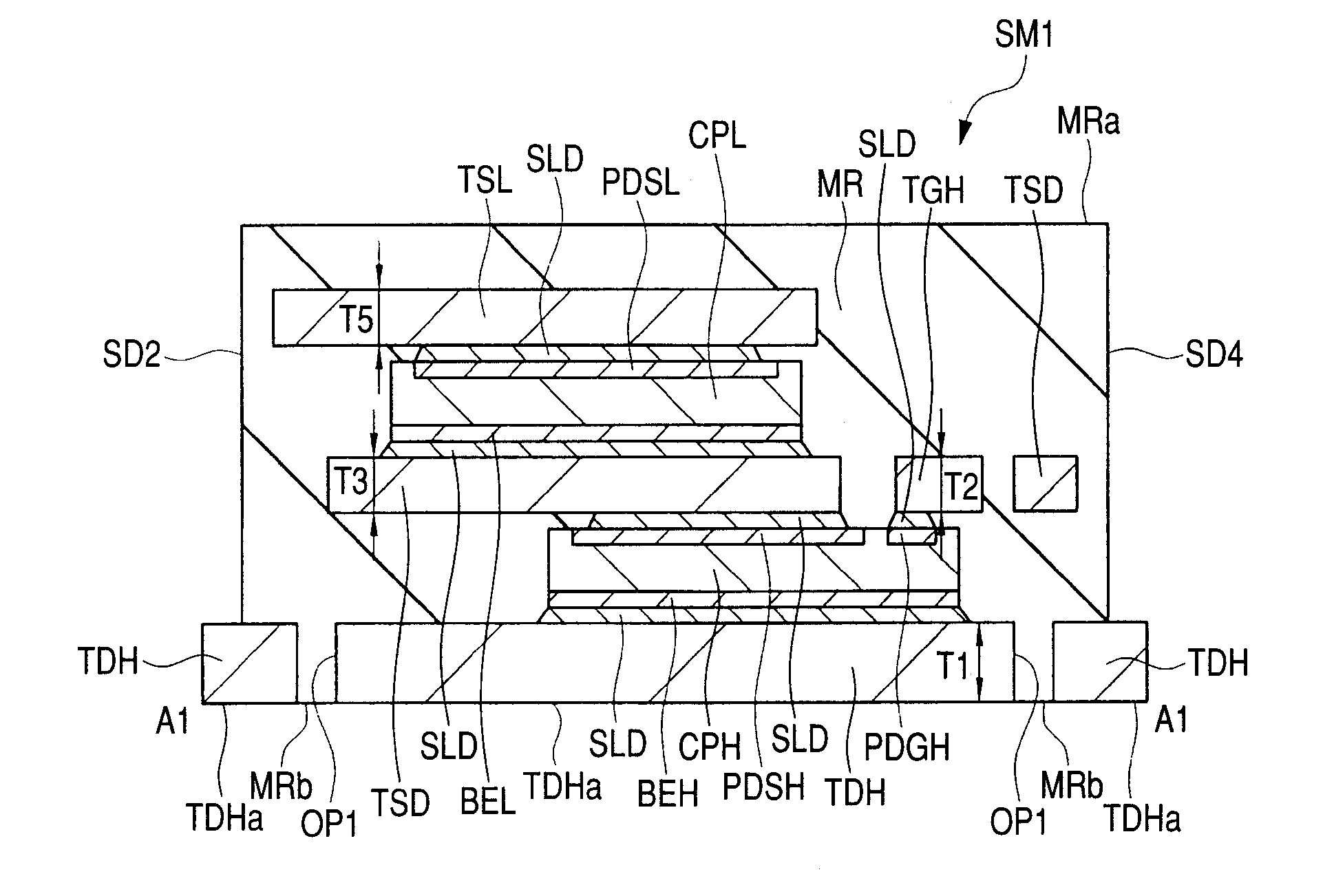
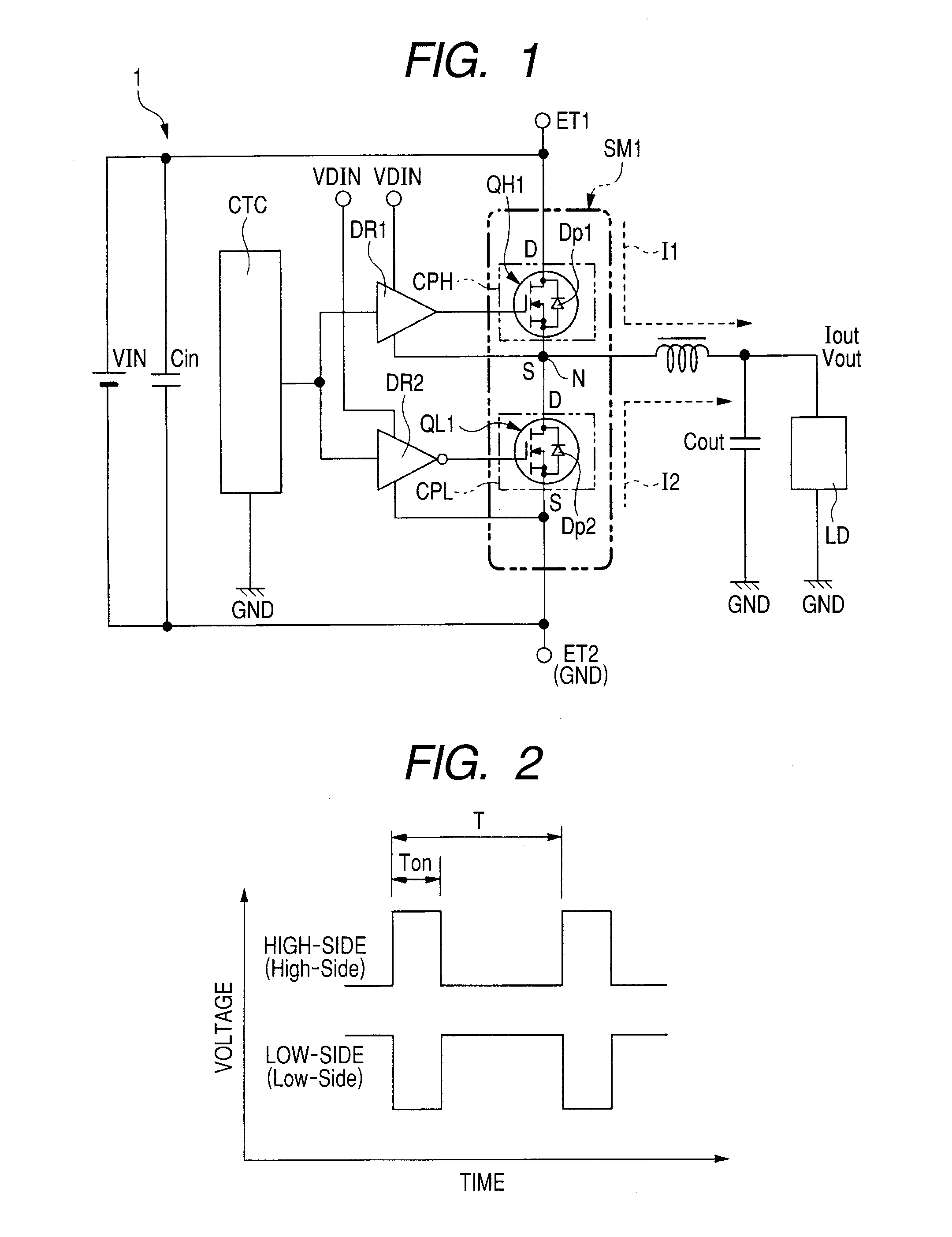
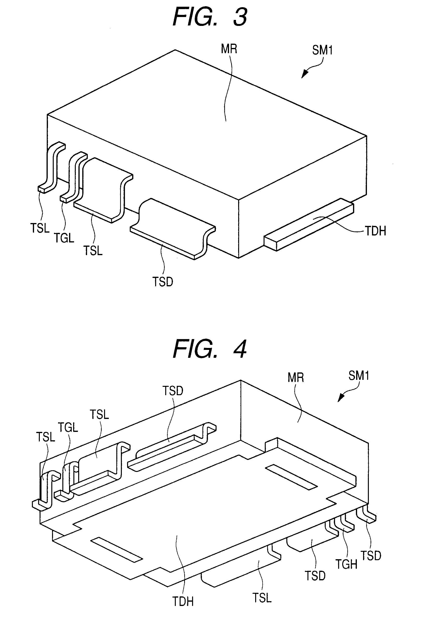
[0138]FIG. 1 is a circuit diagram illustrating an example of a DC-DC converter, non-isolated DC-DC converter (DC-DC converter) 1 in this example, having a semiconductor device (semiconductor package) SM1 in an embodiment of the invention; and FIG. 2 is a basic operating waveform chart of the non-isolated DC-DC converter 1 in FIG. 1.

[0139]This non-isolated DC-DC converter 1 is used in the power supply circuit of an electronic device, such as a desk top personal computer, a notebook personal computer, a server, game machine, or the like. It includes the semiconductor device SM1, two driver circuits (drive circuits) DR1, DR2, a control circuit CTC, an input capacitor Cin, an output capacitor Cout, a...


PUM


Abstract

The reliability of a semiconductor device is enhanced. A first lead frame, a first semiconductor chip, a second lead frame, and a second semiconductor chip are stacked over an assembly jig in this order with solder in between and solder reflow processing is carried out to fabricate their assembly. Thereafter, this assembly is sandwiched between first and second molding dies to form an encapsulation resin portion. The upper surface of the second die is provided with steps. At a molding step, the second lead frame is clamped between the first and second dies at a position higher than the first lead frame; and a third lead frame is clamped between the first and second dies at a higher position. The assembly jig is provided with steps at the same positions as those of the steps in the upper surface of the second die in positions corresponding to those of the same.

Description

CROSS-REFERENCE TO RELATED APPLICATIONS[0001]The disclosure of Japanese Patent Application No. 2009-233125 filed on Oct. 7, 2009 including the specification, drawings and abstract is incorporated herein by reference in its entirety.BACKGROUND OF THE INVENTION[0002]The present invention relates to manufacturing methods for semiconductor devices and in particular to a technology effectively applicable to a manufacturing method for plastic molded semiconductor package-type semiconductor devices.[0003]Various types of semiconductor packages are used and among them there is a plastic molded semiconductor package in which a semiconductor chip is sealed with an encapsulation resin portion. In plastic molded semiconductor packages, a semiconductor chip is sealed in an encapsulation resin portion; therefore, the reliability of the semiconductor chip can be enhanced. When a terminal is exposed in the back surface of the encapsulation resin portion, the plastic molded semiconductor package can...

Claims


Application Information

Patent Timeline
IPC IPC(8): H01L21/60
CPCH01L21/4842H01L23/49537H01L2924/1306H01L2224/0401H01L2224/05556H01L2224/02166H01L2224/33181H01L2224/73253H01L23/49575H01L24/03H01L24/05H01L24/33H01L24/73H01L24/83H01L2224/04042H01L2224/32245H01L2224/838H01L2225/06562H01L2924/01004H01L2924/01005H01L2924/01013H01L2924/01014H01L2924/01015H01L2924/01022H01L2924/01029H01L2924/01075H01L2924/01078H01L2924/01079H01L2924/01082H01L2924/014H01L2924/13091H01L2924/14H01L2924/1433H01L2924/19041H01L2924/30107H01L2224/05H01L2224/2919H01L2924/01006H01L2924/01023H01L2924/01024H01L2924/01033H01L2924/0665H01L2224/16245H01L2924/00H01L2924/181H01L2924/00012
Inventor MACHIDA, YUICHI
Owner RENESAS ELECTRONICS CORP
Why Eureka
Try Eureka