Semiconductor device

a technology of semiconductors and devices, applied in semiconductor/solid-state device testing/measurement, basic electric elements, instruments, etc., can solve the problems of unignorable difference in wiring length between signal paths, incomplete chip replacement, and incomplete chip replacement, etc., to achieve flexible switching and enhance signal quality.

Active Publication Date: 2011-04-14
LONGITUDE LICENSING LTD
View PDF5 Cites 45 Cited by
  • Summary
  • Abstract
  • Description
  • Claims
  • Application Information

AI Technical Summary

Benefits of technology

[0010]According to the present invention, a defective through silicon via is not simply replaced by an auxiliary through silicon via, but the defective through silicon via is bypassed by shifting a connection relation between driver circuits and the through silicon vias and a connection relation between receiver circuits and the through silicon vias can be flexibly switched. Therefore, almost no difference in wiring lengths occurs between signal paths before and after replacement of the through silicon vias. Thus, because almost no skew is generated, the signal quality can be enhanced.

Problems solved by technology

However, the entire chip becomes defective when even one of the through silicon vias becomes defective, and if a plurality of the chips are stacked, all the chips become defective.
However, when a defective through silicon via is simply replaced with an auxiliary through silicon via, an unignorable difference in wiring lengths can occur between signal paths before and after replacement of the through silicon vias depending on a location of the defective through silicon via.
The skew can degrade the signal quality.
This problem is not limited to semiconductor memory devices such as DRAMs, but can occur to all semiconductor devices that include a plurality of semiconductor chips that are electrically connected to each other via through silicon vias.

Method used


Image

  • Semiconductor device
  • Semiconductor device
  • Semiconductor device

Examples


first embodiment

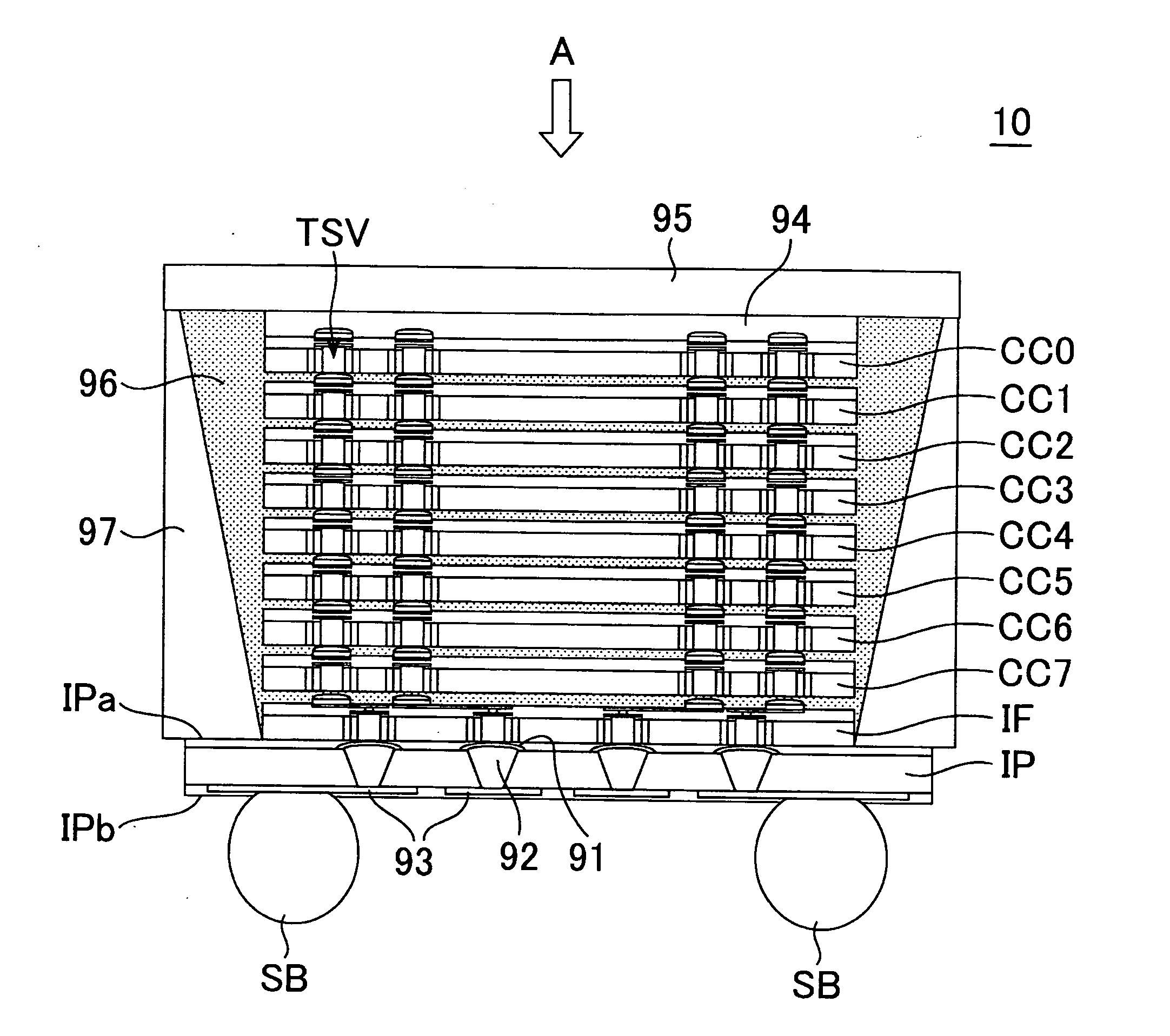
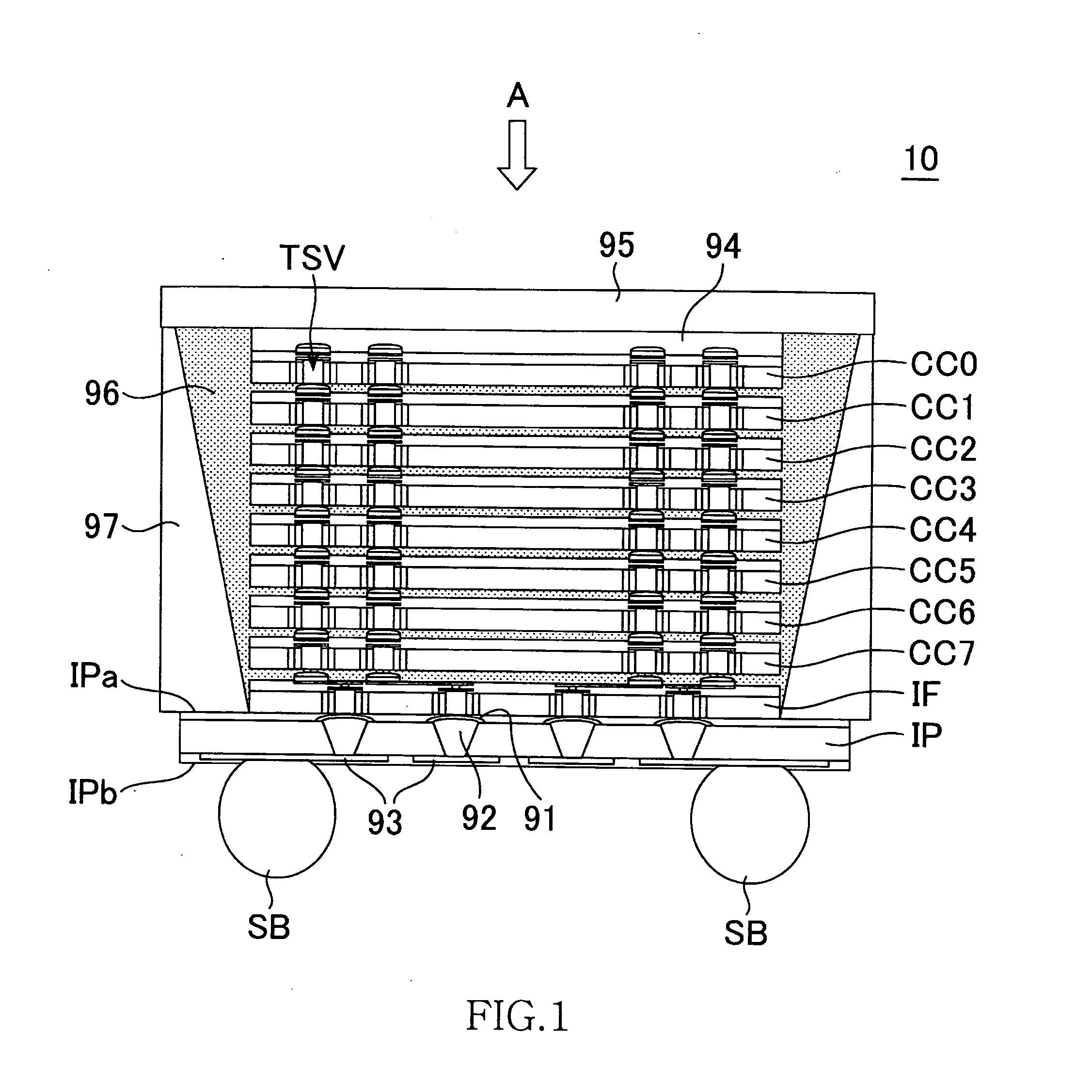
[0037]FIG. 4 is a schematic circuit diagram for explaining a connection relation between the interface chip IF and the core chips CC0 to CC7 according to the present invention. FIG. 4 shows a state where none of the through silicon vias is defective.

[0038]In FIG. 4, as an example, there is shown a portion where 8-bit data D1 to D8 is supplied from the interface chip IF to each of the core chips CC0 to CC7. The data D1 to D8 are signals that need to be simultaneously output from the interface chip IF and simultaneously input into each of the core chips CC0 to CC7. Address signals and write data are examples of such data.

[0039]As shown in FIG. 4, the interface chip IF includes eight driver circuits 101 to 108 corresponding to the data D1 to D8, and each of the core chips CC0 to CC7 includes eight receiver circuits 201 to 208 corresponding to the data D1 to D8. Meanwhile, in the first embodiment, nine (8+1) through silicon vias 301 to 309 are prepared to connect the driver circuits 101...

second embodiment

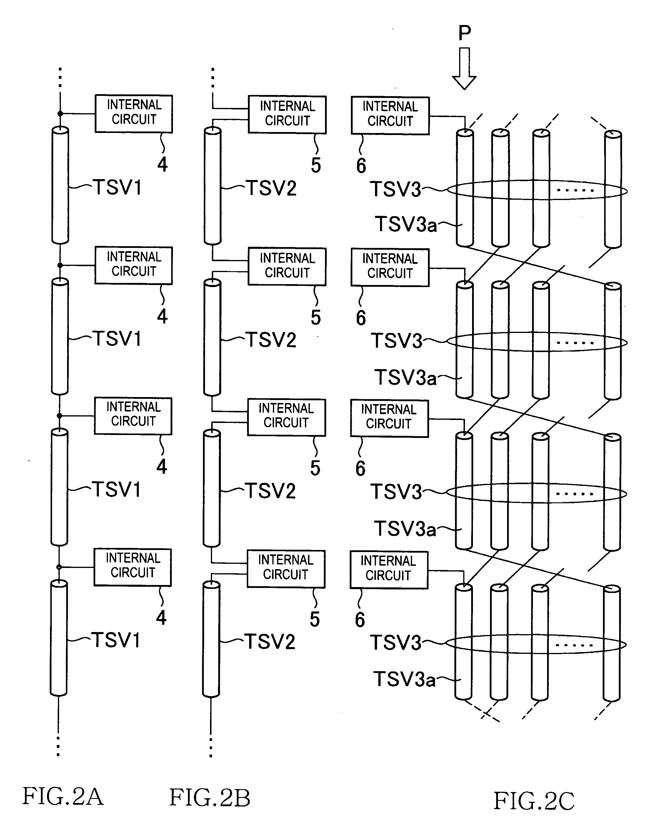
[0061]FIG. 8 is a schematic circuit diagram for explaining a connection relation between the interface chip IF and the core chips CC0 to CC7 according to the present invention, and shows a case where the through silicon vias 302 and 304 are defective.

[0062]As shown in FIG. 8, in the second embodiment, two auxiliary through silicon vias 309 and 310 are allocated with respect to eight through silicon vias 301 to 308. That is, the total number of the through silicon vias is ten.

[0063]In the second embodiment, two output switching circuits 130 and 140 are arranged on an interface chip IF side, and two input switching circuits 230 and 240 are arranged on the core chips CC0 to CC7 side. Relief signals R11 to R18 are supplied to the output switching circuit 130 and the input switching circuit 230, and switching of output paths and input paths is performed based on these relief signals. Similarly, relief signals R21 to R29 are supplied to the output switching circuit 140 and the input switc...


PUM


Abstract

To include a first semiconductor chip including driver circuits, a second semiconductor chip including receiver circuits, and through silicon vias provided in the second semiconductor chip. The first semiconductor chip includes an output switching circuit that exclusively connects an output terminal of an i-th driver circuit (where i is an integer among 1 to n) to one through silicon via among an i-th through silicon via to an (i+m)-th through silicon via. The second semiconductor chip includes an input switching circuit that exclusively connects an input terminal of an i-th receiver circuit (where i is an integer among 1 to n) to one through silicon via among the i-th through silicon via to the (i+m)-th through silicon via. With this configuration, because a difference in wiring lengths does not occur between signal paths before and after replacement of through silicon vias, the signal quality can be enhanced.

Description

BACKGROUND OF THE INVENTION[0001]1. Field of the Invention[0002]The present invention relates to a semiconductor device, and more particularly relates to a semiconductor device including a plurality of semiconductor chips electrically connected by through silicon vias.[0003]2. Description of Related Art[0004]A memory capacity required in semiconductor memory devices such as DRAM (Dynamic Random Access Memory) is increasing every year. In recent years, there has been proposed a method to meet this requirement. In this method, a plurality of memory chips are stacked and electrically connected via through silicon vias arranged on a silicon substrate (see Japanese Patent Application Laid-open No. 2007-158237).[0005]Specifically, in a semiconductor memory device in which an interface chip having front end units such as interface circuits incorporated thereon and a core chip having back end units such as memory cores incorporated thereon are stacked, because read data that is read in para...

Claims


Application Information

Patent Timeline
Patent Type & Authority Applications(United States)
IPC IPC(8): H01L25/00
CPCG11C5/063H01L27/1052G11C29/12G11C29/1201H01L22/22H01L23/481H01L25/0657H01L27/10897H01L2224/16145H01L2225/06513H01L2225/06517H01L2225/06541H01L2225/06596H01L2924/01019H01L2924/01037H01L2924/01055H01L23/5384G11C29/025H10B12/50H10B99/00
Inventor SHIBATA, KAYOKOMIWA, HITOSHIINOUE, YOSHIHIKO
Owner LONGITUDE LICENSING LTD
Why Eureka
Try Eureka