Magnetic Random Access Memory (MRAM) Manufacturing Process for a Small Magnetic Tunnel Junction (MTJ) Design with a Low Programming Current Requirement

a random access memory and manufacturing process technology, applied in the field of nonvolatile magnetic random access memory, can solve the problems of large physical size, high power dissipation, access latency,

Active Publication Date: 2011-04-21
AVALANCHE TECH
View PDF64 Cites 120 Cited by
  • Summary
  • Abstract
  • Description
  • Claims
  • Application Information

AI Technical Summary

Problems solved by technology

Though widely used and commonly accepted, such media suffer from a variety of deficiencies, such as access latency, higher power dissipation, large physical size and inability to withstand any physical shock.
Other dominant storage devices are dynamic random access memory (DRAM) and static RAM (SRAM) which are volatile and very costly but have fast random read/write access time.
Although NAND-based flash memory is more costly than HDD's, it has replaced magnetic hard drives in many applications such as digital cameras, MP3-players, cell phones, and hand held multimedia devices due, at least in part, to its characteristic of being able to retain data even when power is disconnected.
However, as memory dimension requirements are dictating decreased sizes, scalability is becoming an issue because the designs of NAND-based Flash memory and DRAM memory are becoming difficult to scale with smaller dimensions.
For example, NAND-based flash memory has issues related to capacitive coupling, few electrons/bit, poor error-rate performance and reduced reliability due to decreased read-write endurance.
It is believed that NAND flash, especially multi-bit designs thereof, would be extremely difficult to scale below 45 nanometers.
Likewise, DRAM has issues related to scaling of the trench capacitors leading to very complex designs

Method used


Image

  • Magnetic Random Access Memory (MRAM) Manufacturing Process for a Small Magnetic Tunnel Junction (MTJ) Design with a Low Programming Current Requirement
  • Magnetic Random Access Memory (MRAM) Manufacturing Process for a Small Magnetic Tunnel Junction (MTJ) Design with a Low Programming Current Requirement
  • Magnetic Random Access Memory (MRAM) Manufacturing Process for a Small Magnetic Tunnel Junction (MTJ) Design with a Low Programming Current Requirement

Examples


Embodiment Construction

[0047]To overcome the limitations in the prior art described above, and to overcome other limitations that will become apparent upon reading and understanding the present specification, the present invention discloses a manufacturing method for magnetic memory cells yielding a small MTJ design with a low programming current requirement.

[0048]These and various other advantages and features of novelty which characterize the invention are pointed out with particularity in the claims annexed hereto and form a part hereof. However, for a better understanding of the invention, its advantages, and the objects obtained by its use, reference should be made to the drawings which form a further part hereof, and to accompanying descriptive matter, in which there are illustrated and described specific examples of embodiments of the present invention.

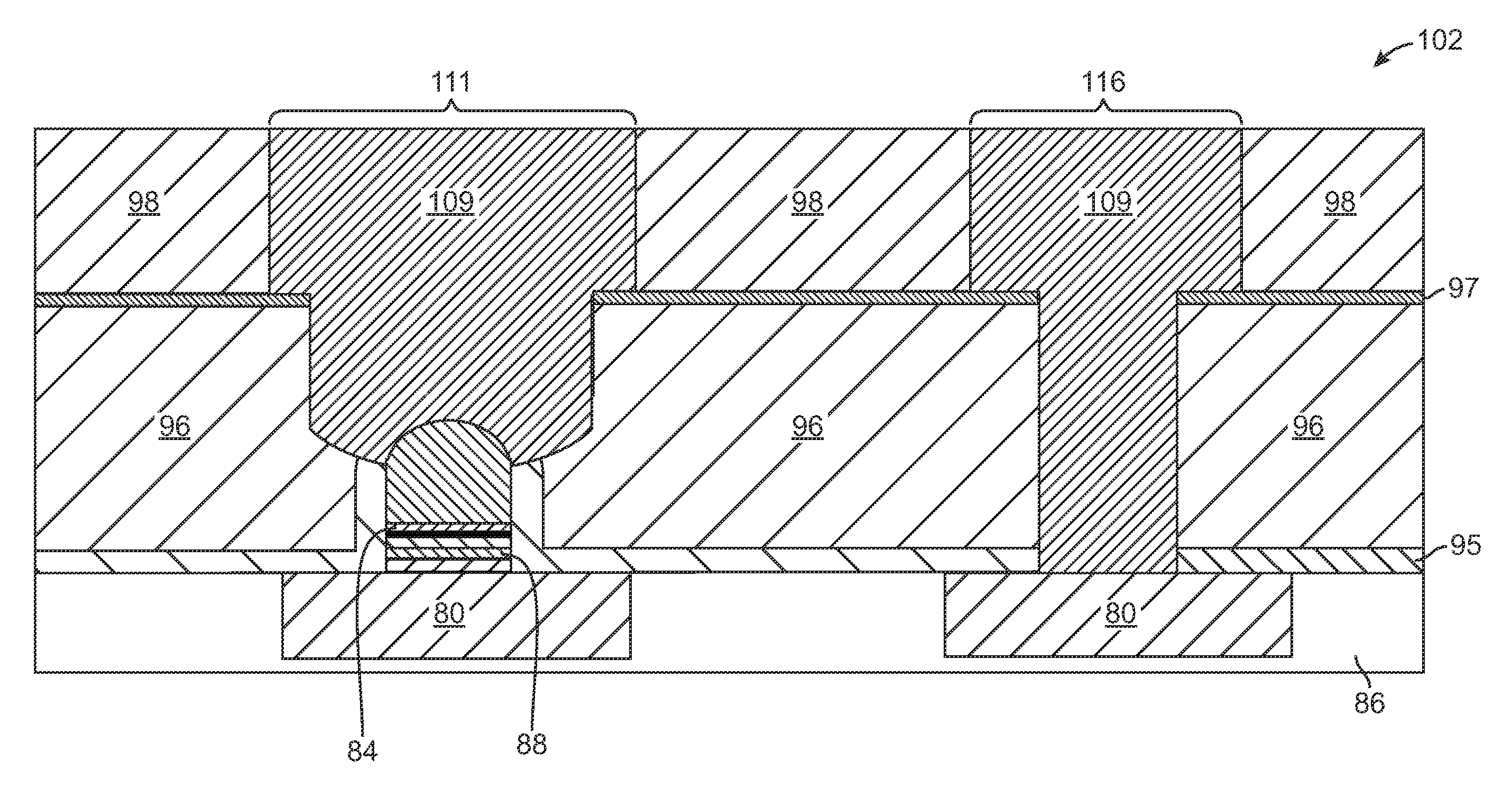
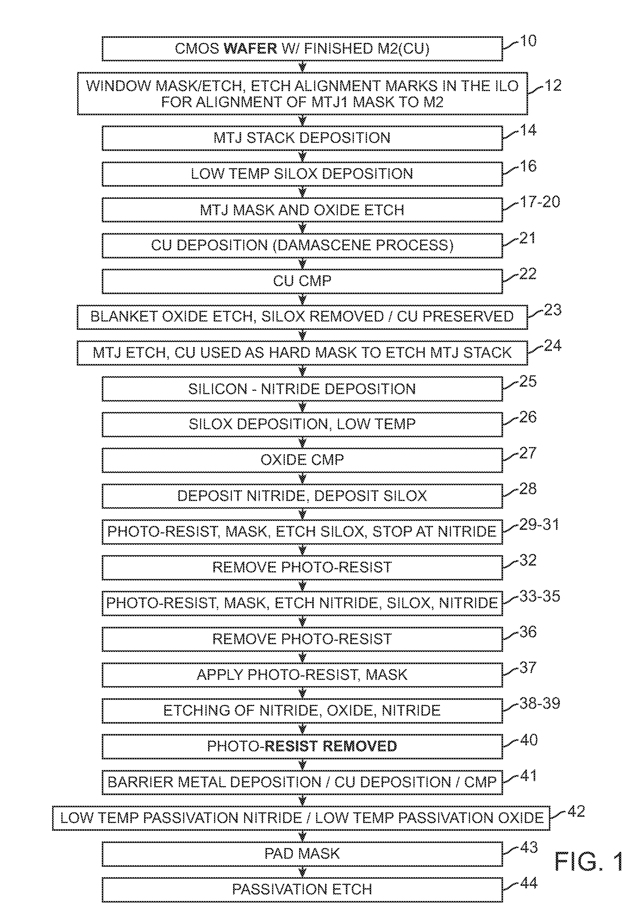
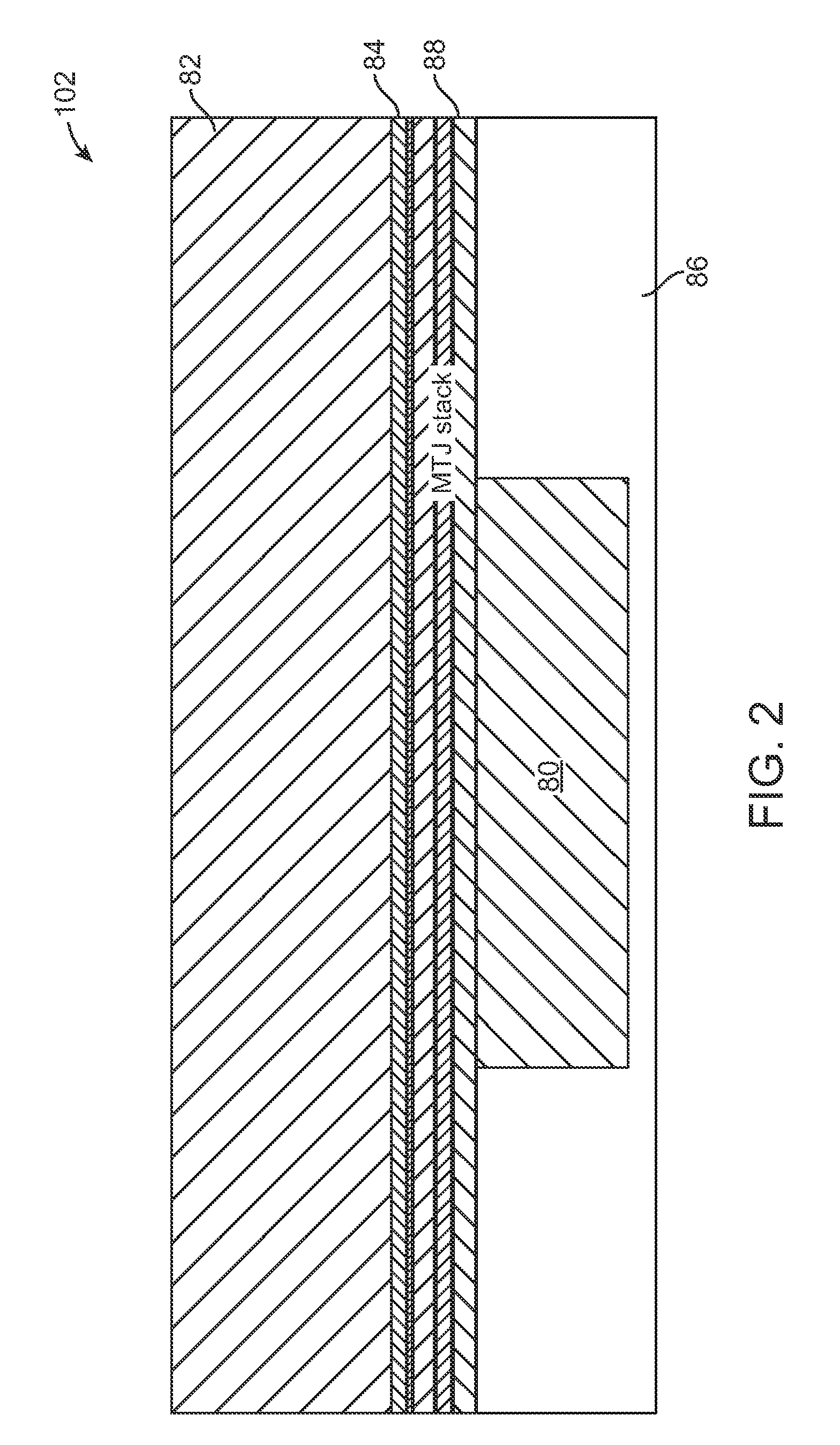
[0049]Referring now to FIG. 1, shows a flow-chart of the MRAM manufacturing process 100 used to manufacture magnetic memory cells. In manufacturing ...


PUM


Abstract

A method of making a magnetic random access memory cell includes forming a magnetic tunnel junction (MTJ) on top of a wafer, depositing oxide on top of the MTJ, depositing a photo-resist layer on top of the oxide layer, forming a trench in the photo-resist layer and oxide layer where the trench has a width that is substantially the same as that of the MTJ. Then, the photo-resist layer is removed and a hard mask layer is deposited on top of the oxide layer in the trench and the wafer is planarized to remove the portion of the hard mask layer that is not in the trench to substantially level the top of oxide layer and the hard layer on the wafer. The remaining oxide layer is etched and the the MTJ is etched to remove the portion of the MTJ which is not covered by the hard mask layer.

Description

CROSS REFERENCE TO RELATED APPLICATIONS[0001]This application is a continuation-in-application of U.S. patent application Ser. No. 11 / 674,124, entitled “Non-Uniform Switching Based Non-Volatile Magnetic Based Memory,” filed Feb. 12, 2007, by Ranjan, et al.; U.S. patent application Ser. No. 11 / 678,515, entitled “A High Capacity Low Cost Multi-State Magnetic Memory,” filed Feb. 23, 2007, by Ranjan, et al.; and U.S. patent application Ser. No. 11 / 776,692, entitled “Non-Volatile Magnetic Memory Element with Graded Layer,” filed Jul. 12, 2007, by Ranjan et al., all of which are incorporated herein by reference as though set forth in full.FIELD OF THE INVENTION[0002]The present invention relates generally to non-volatile magnetic random access memory and particularly to a method for manufacturing memory cells for non-volatile magnetic random access memory incorporating a small magnetic tunnel junction (MTJ).DESCRIPTION OF THE PRIOR ART[0003]Computers conventionally use rotating magnetic m...

Claims


Application Information

Patent Timeline
IPC IPC(8): H01L29/82H01L21/8246
CPCB82Y10/00G11C11/16H01L43/12H01L43/08H01L27/228G11C11/161H10B61/22H10N50/10H10N50/01
Inventor KESHTBOD, PARVIZMALMHALL, ROGER KLASRANJAN, RAJIV YADAV
Owner AVALANCHE TECH
Why Eureka
Try Eureka