Area reduction for electrical diode chips
- Summary
- Abstract
- Description
- Claims
- Application Information
AI Technical Summary
Benefits of technology
Problems solved by technology
Method used
Image

Examples
Embodiment Construction
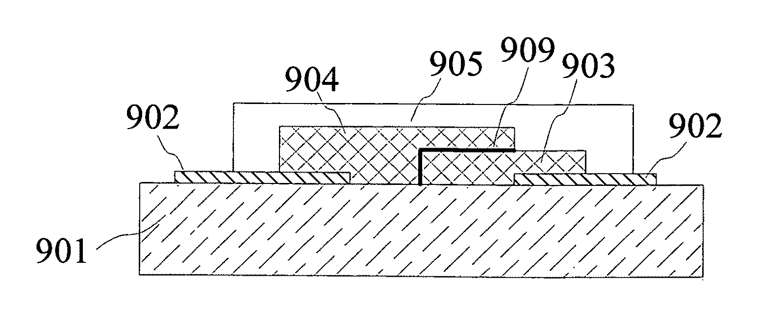
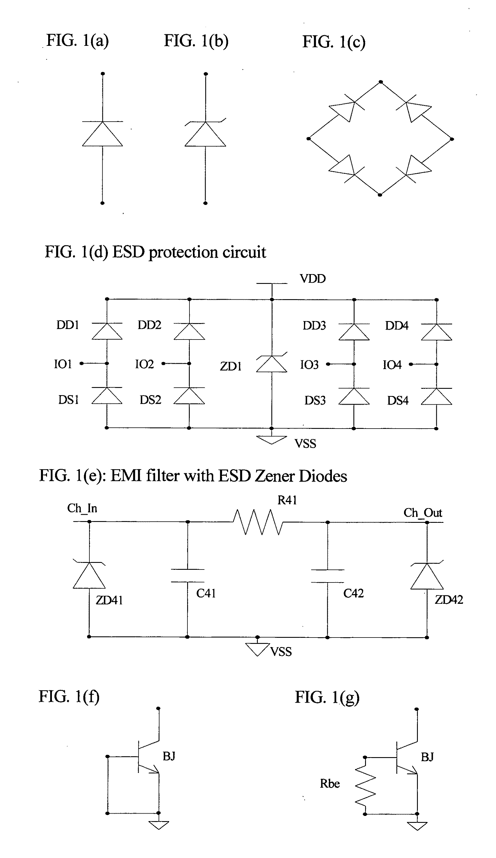
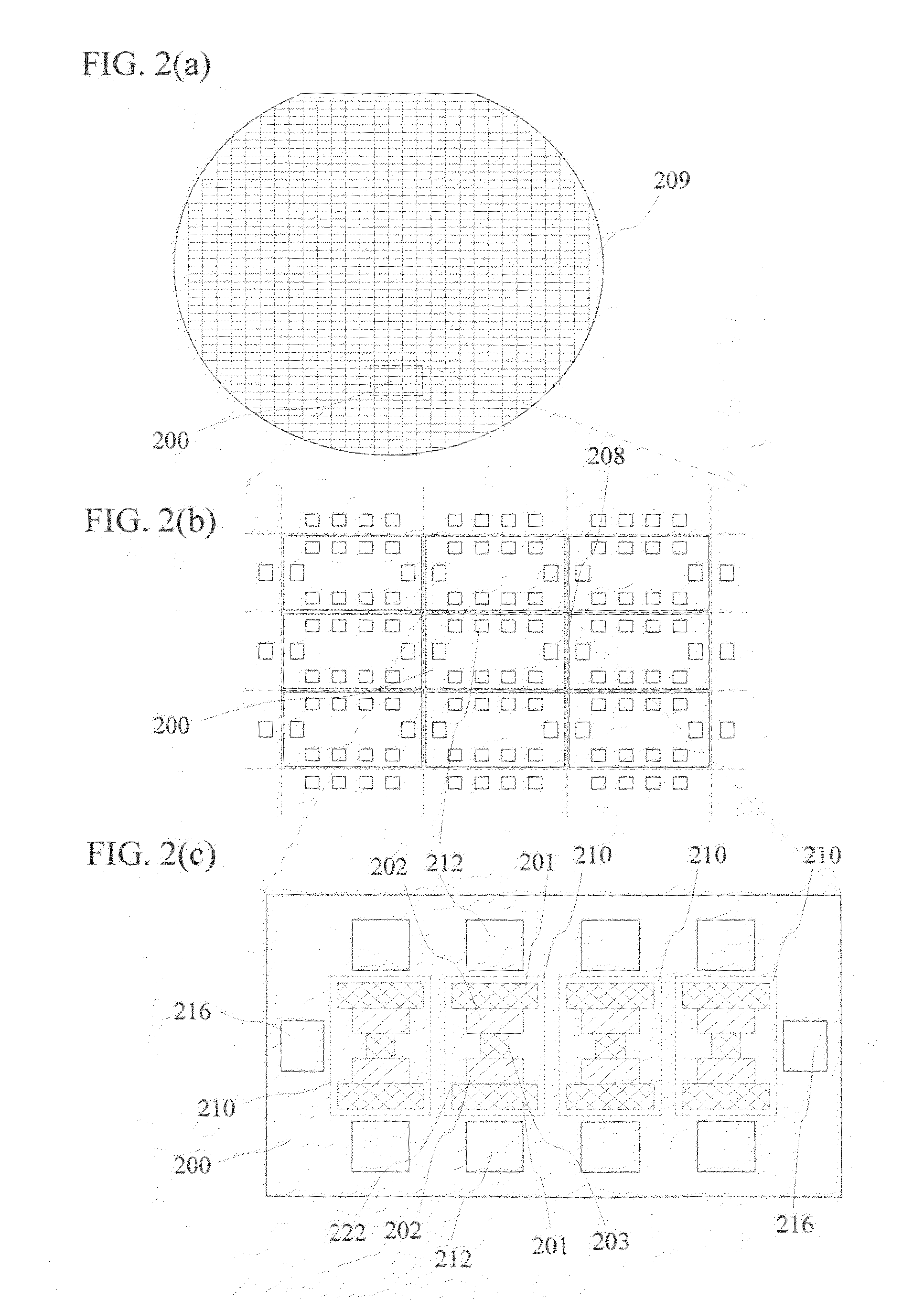
[0023]The primary objective of our preferred embodiment is, therefore, to reduce the area of ESD protection chips or electrical diode chips. The other objective of our preferred embodiment is to provide cost effective external ESD protection chips or electrical diode chips. The other objective of our preferred embodiment is to reduce the parasitic inductance on the I / O connections of external ESD protection chips or electrical diode chips. These and other objectives are achieved by patterning conductor leads of ESD protection chips or electrical diode chips using dried-ink conductors patterned by printing processes.
[0024]While the novel features of the invention are set forth with particularly in the appended claims, our preferred embodiments, both as to organization and content, will be better understood and appreciated, along with other objects and features thereof, from the following detailed description taken in conjunction with the drawing.
BRIEF DESCRIPTION OF THE DRAWINGS
[0025...
PUM
 Abstract
Description
Claims
Application Information