Light emitting device and manufacturing method therefor

a technology of light emitting diodes and manufacturing methods, which is applied in semiconductor devices, electric lighting sources, electric light sources, etc., can solve the problems of high manufacturing cost and difficulty in manufacturing itself, and achieve the effect of reducing manufacturing costs and simplifying the manufacturing process

Inactive Publication Date: 2011-04-21
SHARP KK
View PDF20 Cites 56 Cited by
  • Summary
  • Abstract
  • Description
  • Claims
  • Application Information

AI Technical Summary

Benefits of technology

[0105]According to the light emitting device of this invention, since the plurality of light emitting diodes to be connected in parallel do not need to be arrayed with their polarity uniformized, the step for uniformizing the polarity (orientation) of the plurality of light emitting diodes becomes unnecessary during the manufacture, thus allowing the manufacturing process to be simplified. Further, since there is no need for providing marks on the light emitting diodes for discrimination of the polarity (orientation) of the light emitting diodes, it also becomes unnecessary to form the light emitting diodes into any special shape. Therefore, the manufacturing process of the light emitting diodes can be simplified, and the manufacturing cost can also be cut down.
[0106]According to the light emitting device of the invention, the first-conductive-type first region and the first-conductive-type third region are placed on both sides of the second-conductive-type second region of the rod-like light emitting element. Therefore, even if connection of the first, third regions of the rod-like light emitting element relative to the first, third electrodes is reversed, the diode polarity is not changed, so that it is possible to fulfill normal light emission. Therefore, the connection of the first, third regions relative to the first, third electrodes during the manufacturing process may be reversed, allowing a simplification of the manufacturing process as well as a cutdown of the manufacturing cost to be achieved.

Problems solved by technology

However, with the first conventional light emitting device, because of the need for connecting plurality of light emitting diodes 101 in parallel with their polarity uniformized, the manufacturing cost goes high particularly with small decreasing sizes of the light emitting diodes or with increasing numbers of connected light emitting diodes, leading to a difficulty in manufacture itself.

Method used


Image

  • Light emitting device and manufacturing method therefor
  • Light emitting device and manufacturing method therefor
  • Light emitting device and manufacturing method therefor

Examples


first embodiment

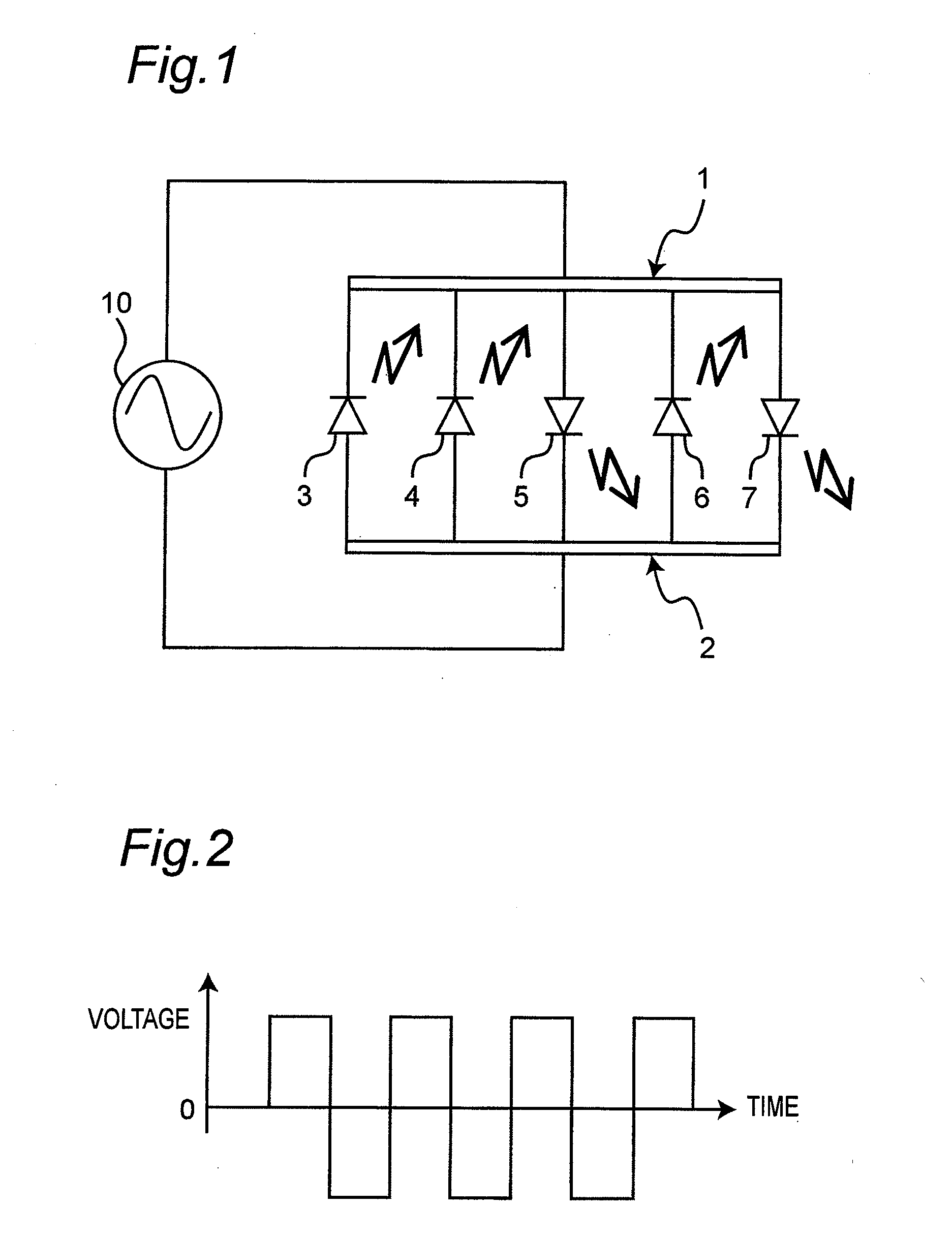
[0134]FIG. 1 schematically shows an electric circuit structure of a first embodiment of a light emitting device according to the present invention. The light emitting device of this first embodiment includes a first electrode 1 and a second electrode 2, and five light emitting diodes 3-7 connected in parallel between the first electrode 1 and the second electrode 2. The light emitting diodes 3, 4, 6 are each a second light emitting diode whose cathode is connected to the first electrode 1 and whose anode is connected to the second electrode 2. Meanwhile, the light emitting diodes 5, 7 are each a first light emitting diode whose anode is connected to the first electrode 1 and whose cathode is connected to the second electrode 2. An AC power supply 10 is connected to the first electrode 1 and the second electrode 2, and the AC power supply 10 applies AC voltage to the first electrode 1 and the second electrode 2. In this embodiment, the frequency of the AC voltage by the AC power supp...

second embodiment

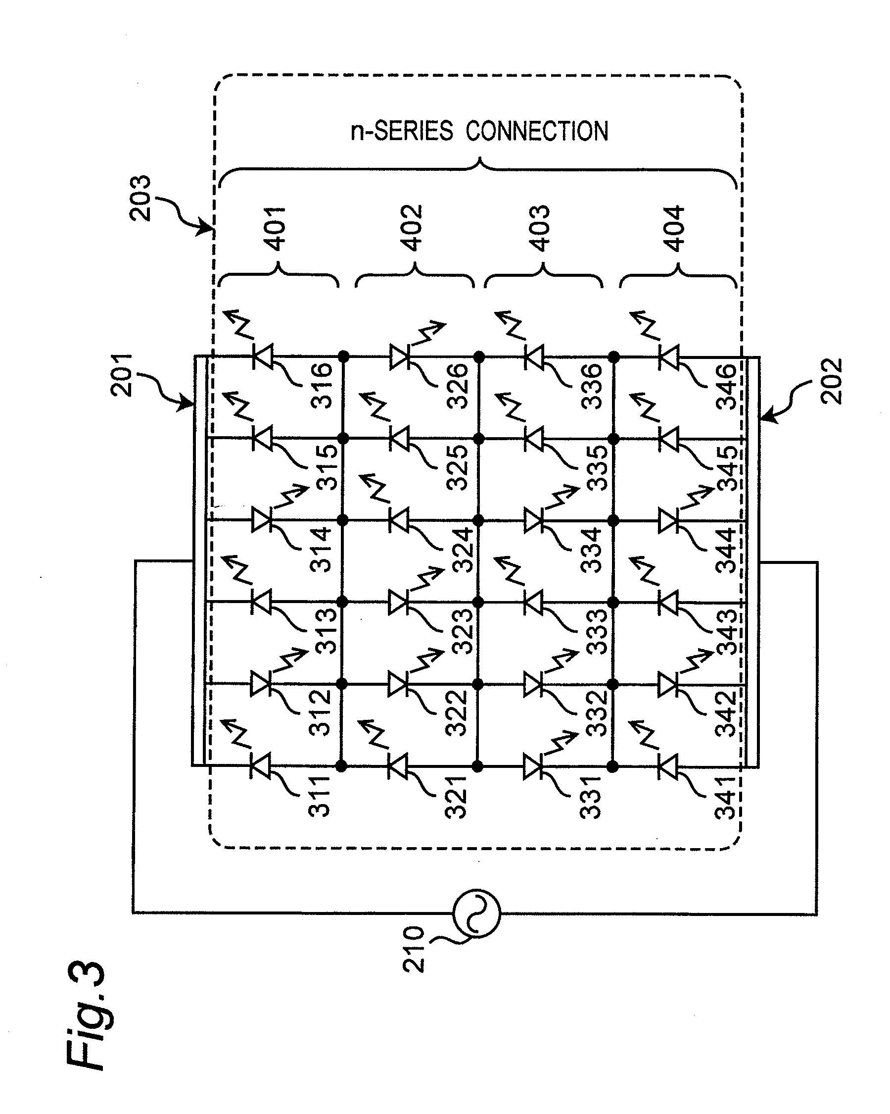
[0144]Next, a second embodiment of the light emitting device according to the invention will be described with reference to FIG. 3. FIG. 3 is a circuit diagram schematically showing an electric circuit structure of the second embodiment.

[0145]FIG. 3 schematically shows the electric circuit structure of the second embodiment of the light emitting device according to the invention. The light emitting device of this second embodiment includes a first electrode 201 and a second electrode 202, and a light emitting diode circuit 203 composed of twenty-four light emitting diodes 311-316, 321-326, 331-336, 341-346 connected in series and parallel between the first electrode 201 and the second electrode 202.

[0146]The six light emitting diodes 311-316 are connected in parallel to form a parallel structure unit 401. Likewise, the six light emitting diodes 321-326, the six light emitting diodes 331-336 and the six light emitting diodes 341-346 also form parallel structure units 402, 403, 404, r...

third embodiment

[0165]Next, a third embodiment of the light emitting device according to the invention will be described with reference to FIG. 7. FIG. 7 is a schematic plan view showing the third embodiment.

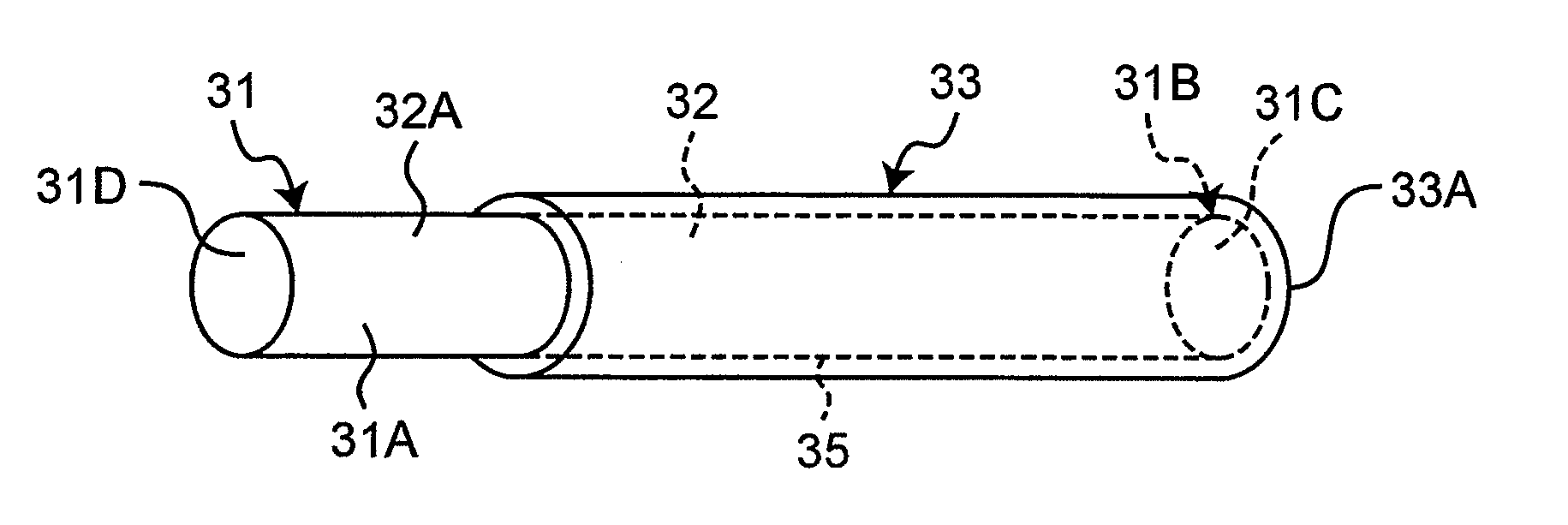
[0166]The light emitting device of this third embodiment includes a substrate 21, a first electrode 22 formed on the substrate 21, a second electrode 23 formed on the substrate 21, and four light emitting diodes 24, 25, 26, 27. These first electrode 22 and the second electrode 23 extend generally parallel to each other along a surface 21A of the substrate 21 and are opposed to each other. The first electrode 22 has four protruding portions 22A, 22B, 22C, 22D which are positioned in parallel to one another with a certain interval along the extending direction of the first electrode 22 and which protrude toward the second electrode 23. Also, the second electrode 23 has four protruding portions 23A, 23B, 23C, 23D which are positioned in parallel to one another with a certain interval along the ext...


PUM


Abstract

In a light emitting device, a P-type first region (506) and a P-type third region (508) are placed on both sides of an N-type second region (507) of a rod-like light emitting element (505). Therefore, even if connection of the first, third regions (506, 508) of the rod-like light emitting element (505) relative to the first, third electrodes (1, 3) is reversed, a diode polarity relative to the first, third electrodes (501, 503) is not reversed, making it possible to effectuate normal light emission. Thus, a connection of the first, third regions (506, 508) relative to the first, third electrodes (501, 503) may be reversed during a manufacturing process, making it unnecessary to provide marks or configurations for discrimination of orientation of the rod-like light emitting element (505), so that the manufacturing process can be simplified and manufacturing cost can be cut down.

Description

TECHNICAL FIELD[0001]The present invention relates to a light emitting device, as well as a manufacturing method therefor, which allows its manufacturing cost to be cut down.BACKGROUND ART[0002]As a first conventional light emitting device, heretofore, there has been provided a light emitting device in which a plurality of light emitting diodes are connected in parallel with their polarity uniformized, and driven by DC current (see Patent Literature 1: JP 2007-134430 A). A simplified circuit of this light emitting device is shown in FIG. 17. In the first conventional light emitting device shown in FIG. 17, a plurality of light emitting diodes 101 are connected in parallel so as to be uniform in polarity, and driven by DC current.[0003]However, with the first conventional light emitting device, because of the need for connecting plurality of light emitting diodes 101 in parallel with their polarity uniformized, the manufacturing cost goes high particularly with small decreasing sizes...

Claims


Application Information

Patent Timeline
Patent Type & Authority Applications(United States)
IPC IPC(8): H05B37/02H01L33/00H01L33/36
CPCH05B33/0803H05B33/0821H05B33/0806H05B45/00H05B45/42H05B45/40H05B45/44
Inventor SHIBATA, AKIHIDENEGISHI, TETSUMORISHITA, SATOSHIKOMIYA, KENJIIWATA, HIROSHITAKAHASHI, AKIRAYAOI, YOSHIFUMI
Owner SHARP KK
Why Eureka
Try Eureka