

Logic circuit and semiconductor device
a logic circuit and semiconductor technology, applied in the field of logic circuits, can solve problems such as malfunction, output signal fluctuation, leakage current generation in some cases, etc., and achieve the effects of reducing leakage current, suppressing malfunction, and reducing leakage curren
- Summary
- Abstract
- Description
- Claims
- Application Information
AI Technical Summary
Benefits of technology
Problems solved by technology
Method used
Image

Examples
embodiment 1
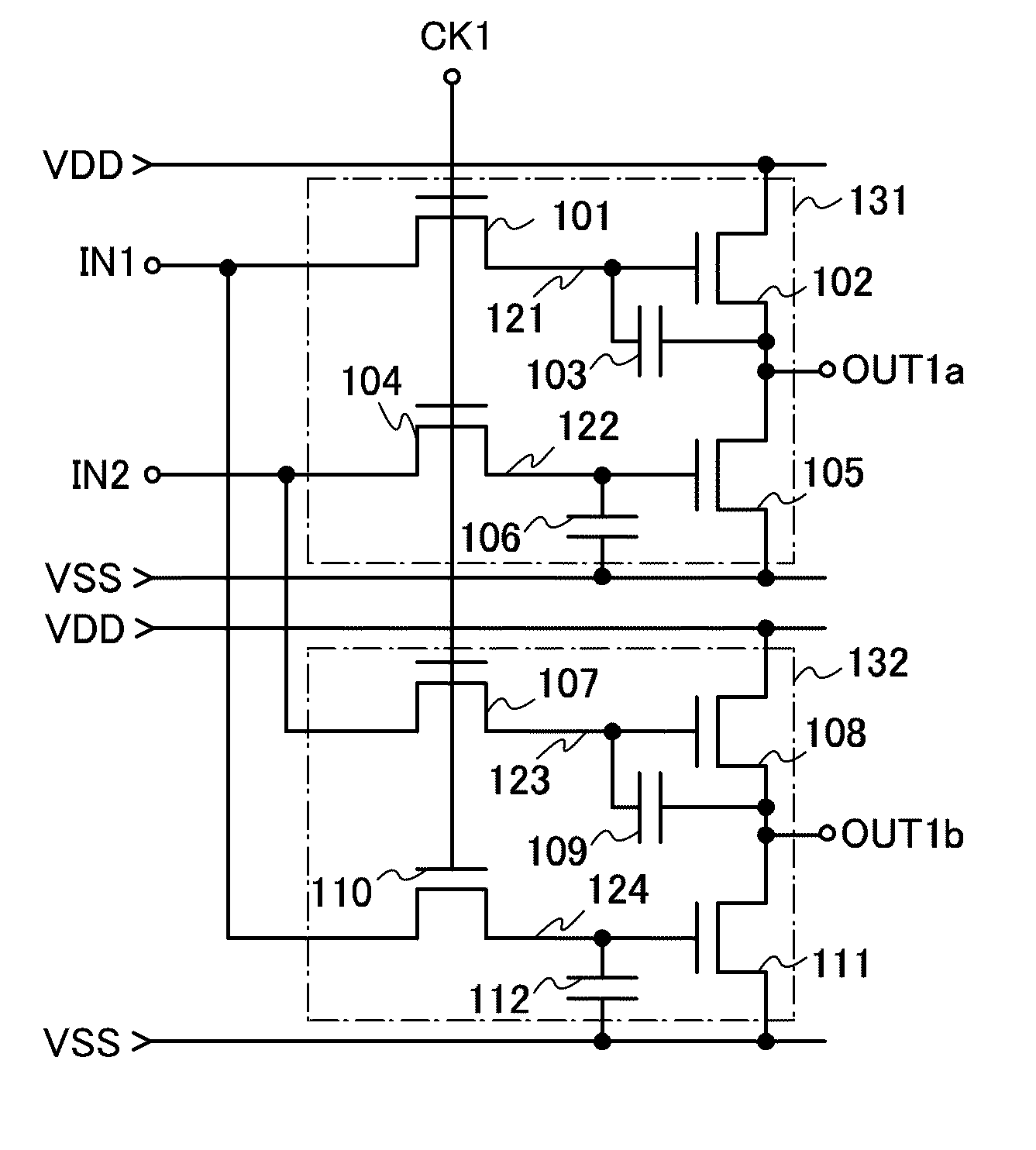
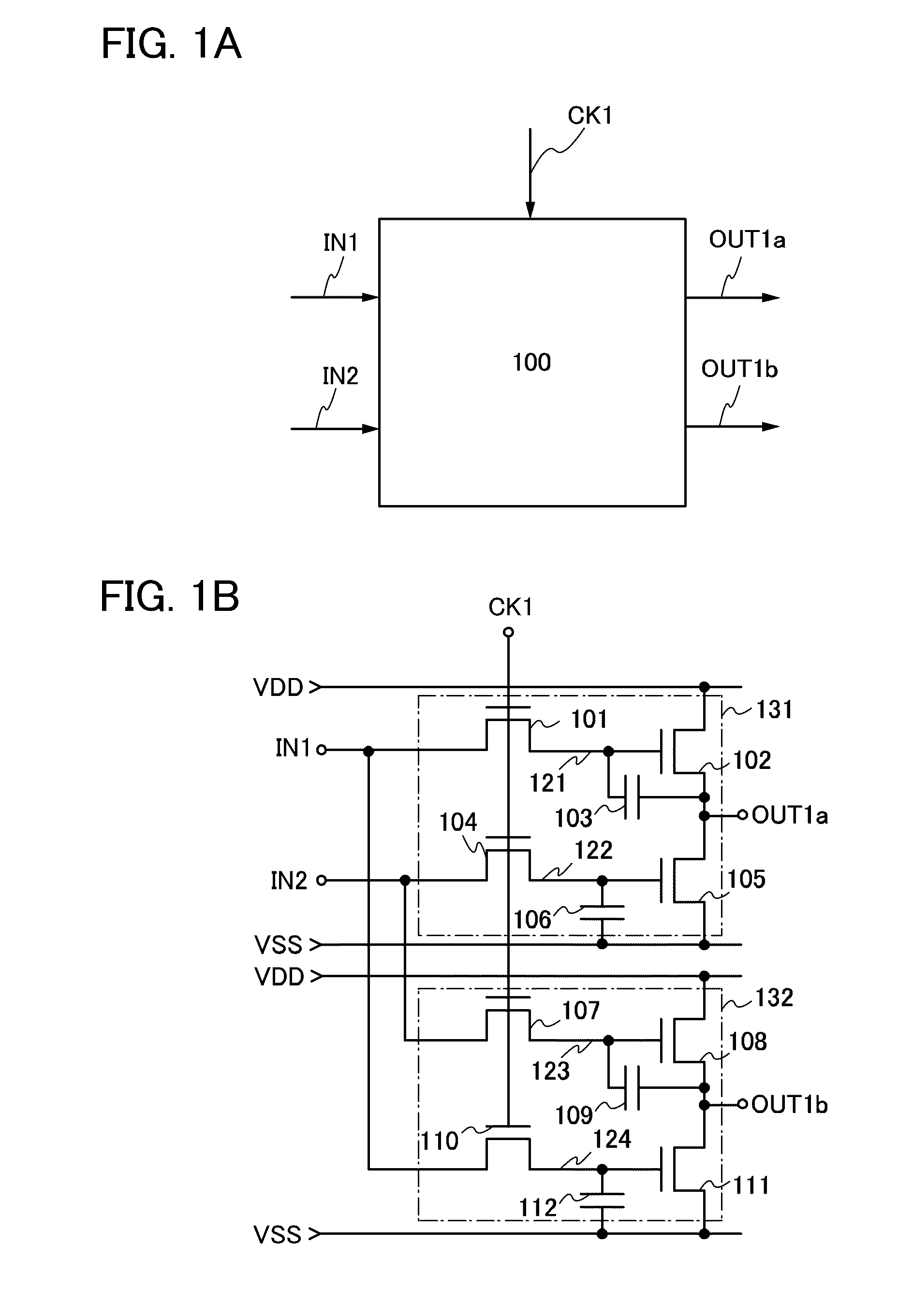
[0051]In this embodiment, a logic circuit which is an embodiment of the present invention is described first. In this specification, a logic circuit includes a combinational logic circuit where a state of an output signal at some point in time is determined by a state of an input signal at the point in time except in the specified case and a sequential logic circuit where a state of an output signal at some point in time is determined by not only a state of an input signal at the point in time but also a state of the sequential logic circuit at the time before the point in time in its category.
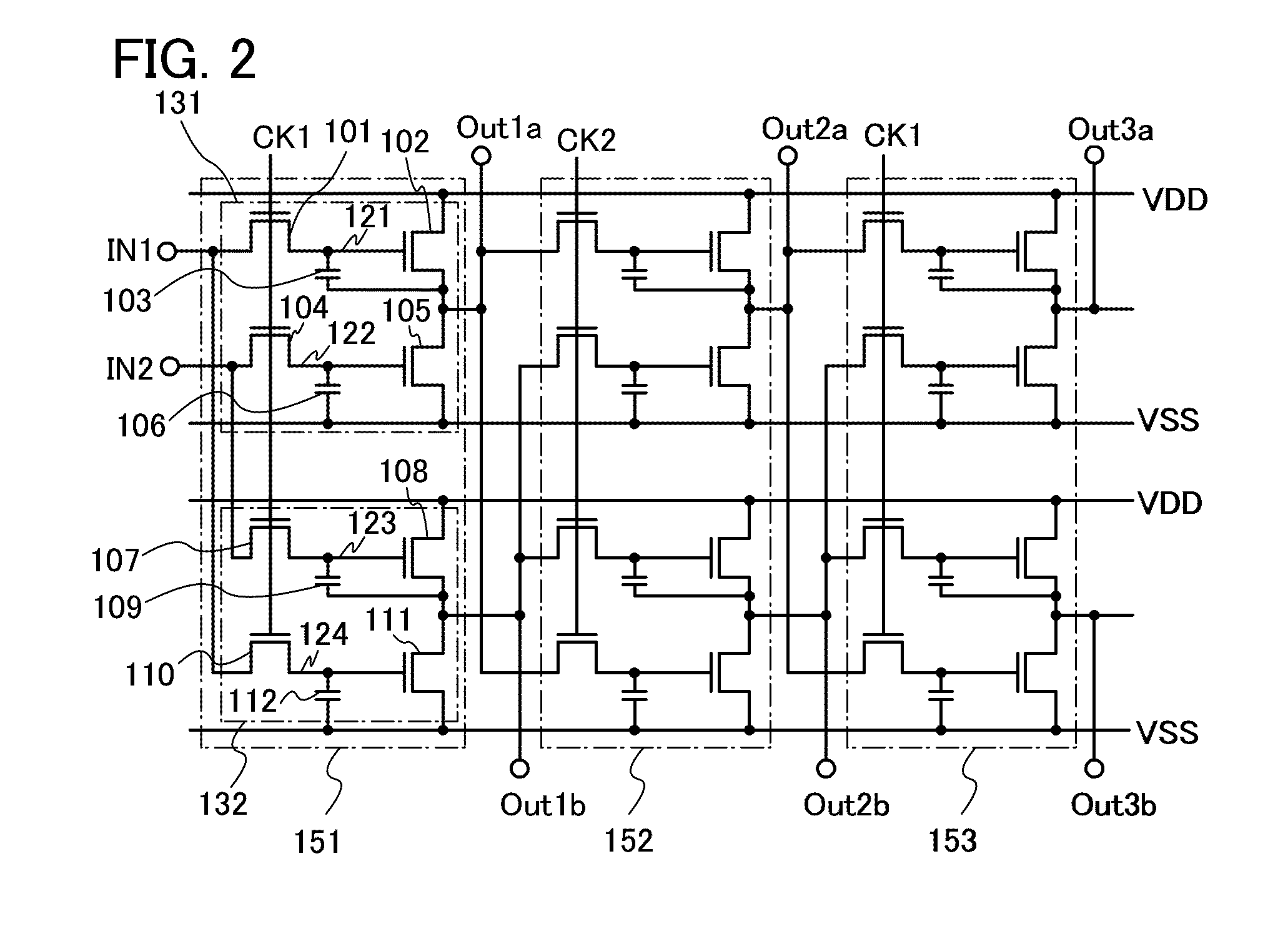
[0052]An example of a configuration of a logic circuit in this embodiment is described with reference to FIGS. 1A and 1B. FIGS. 1A and 1B illustrate an example of a configuration of a logic circuit in this embodiment.
[0053]To a logic circuit 100 in FIG. 1A, signals IN1, IN2, and CK1 are input as input signals. The logic circuit 100 in FIG. 1A outputs signals OUT1a and OUT1b as output signals.
[...
embodiment 2
[0135]In this embodiment, an example of thin film transistors which can be applied to transistors included in the logic circuit and the semiconductor device disclosed in this specification.
[0136]One embodiment of a semiconductor device and a manufacturing method of the semiconductor device of this embodiment is described with reference to FIGS. 31A and 31B and FIGS. 6A to 6E.
[0137]FIGS. 31A and 31B illustrate an example of a planar structure and a cross-sectional structure of a semiconductor device. A thin film transistor 410 illustrated in FIGS. 31A and 31B is one of top gate thin film transistors.
[0138]FIG. 31A is a plan view of the thin film transistor 410 having a top-gate structure and FIG. 31B is a cross-sectional view taken along C1-C2 in FIG. 31A.
[0139]The thin film transistor 410 includes, over a substrate 400, an insulating layer 407, an oxide semiconductor layer 412, a source or drain electrode layer 415a, a source or drain electrode layer 415b, a gate insulating layer 40...
embodiment 3
[0207]In this embodiment, another example of thin film transistors which can be applied to transistors included in the logic circuit and the semiconductor device disclosed in this specification. The same portions as those in Embodiment 2 and portions having functions similar to those of the portions in Embodiment 2 and steps similar to those in Embodiment 2 may be handled as in Embodiment 2, and repeated description is omitted. In addition, detailed description of the same portions is also omitted.
[0208]One embodiment of a semiconductor device and a manufacturing method of the semiconductor device of this embodiment is described with reference to FIGS. 7A and 7B and FIGS. 8A to 8E.
[0209]FIGS. 7A and 7B illustrate an example of a planar structure and a cross-sectional structure of a semiconductor device. A thin film transistor 460 illustrated in FIGS. 7A and 7B is one of top gate thin film transistors.
[0210]FIG. 7A is a plan view of the thin film transistor 460 having a top-gate stru...
PUM
 Abstract
Description
Claims
Application Information