Method for manufacturing and testing an integrated electronic circuit

Active Publication Date: 2011-04-21
STMICROELECTRONICS (GRENOBLE 2) SAS
View PDF6 Cites 18 Cited by
  • Summary
  • Abstract
  • Description
  • Claims
  • Application Information

AI Technical Summary

Benefits of technology

[0012]There thus is a need for an integrated circuit manufacturing

Problems solved by technology

This pressing has the disadvantage of forming, on the contact pads, scratches which may raise problems of reliability of the connection elements formed on the contact pads.
However, the use of contact pads formed of two elementary pads, and thus having a relatively lar

Method used


Image

  • Method for manufacturing and testing an integrated electronic circuit
  • Method for manufacturing and testing an integrated electronic circuit
  • Method for manufacturing and testing an integrated electronic circuit

Examples


Example

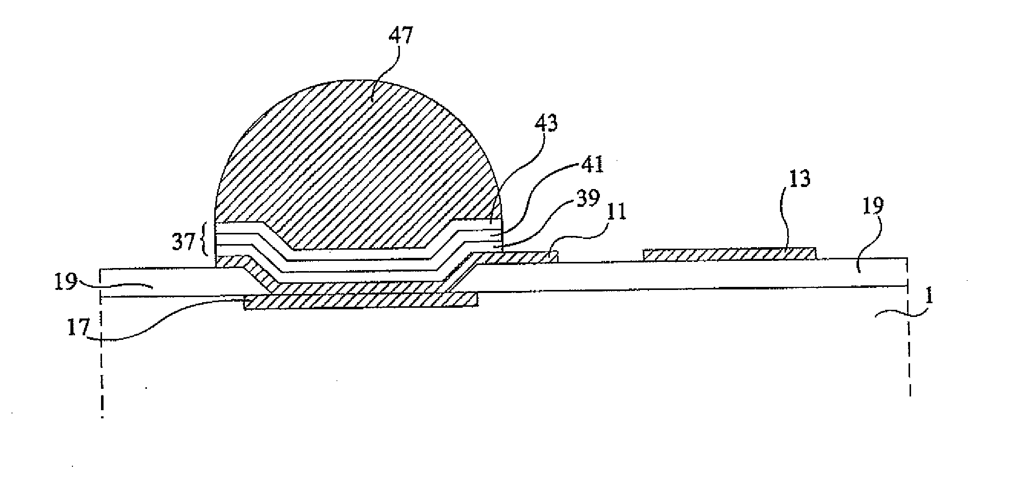
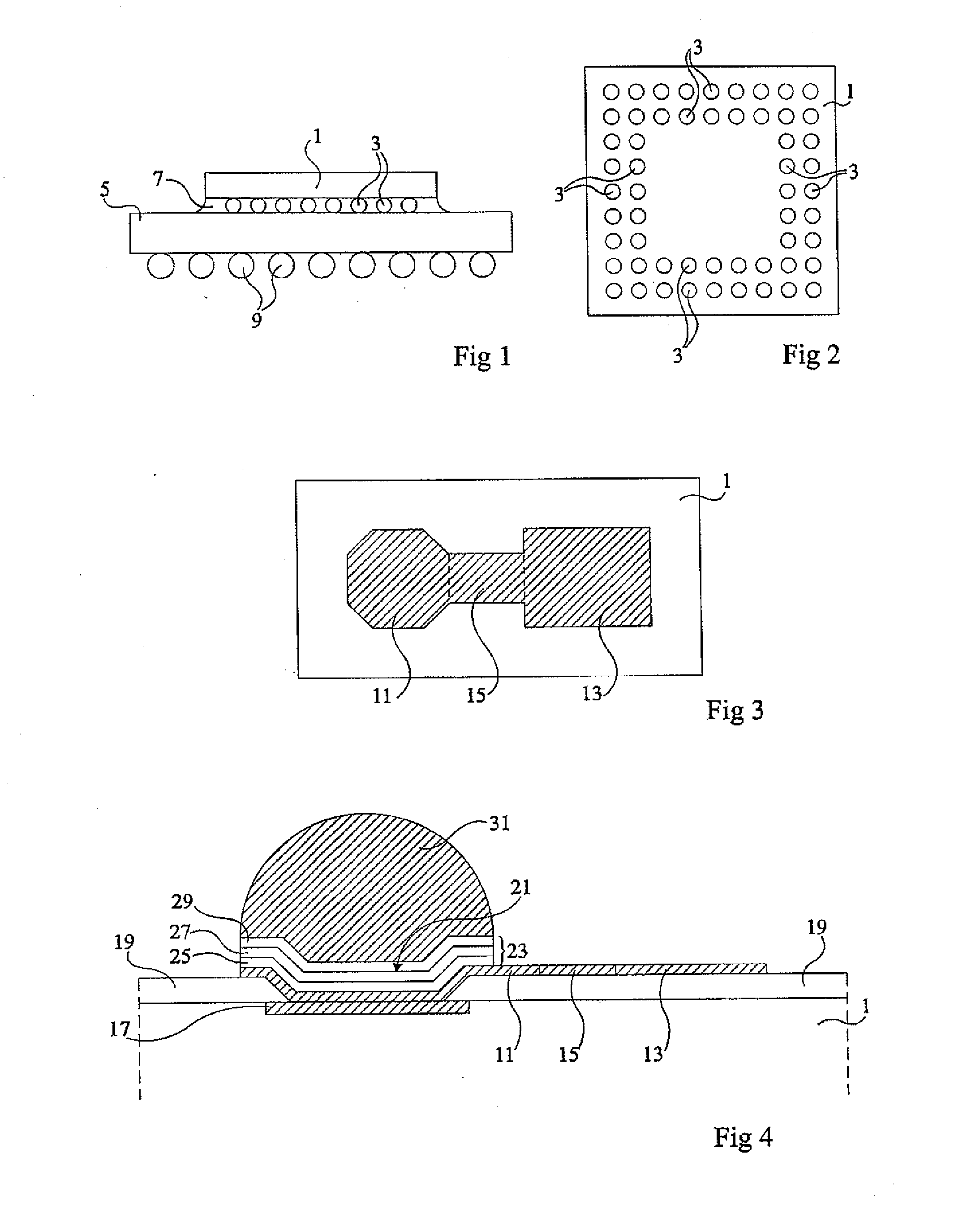
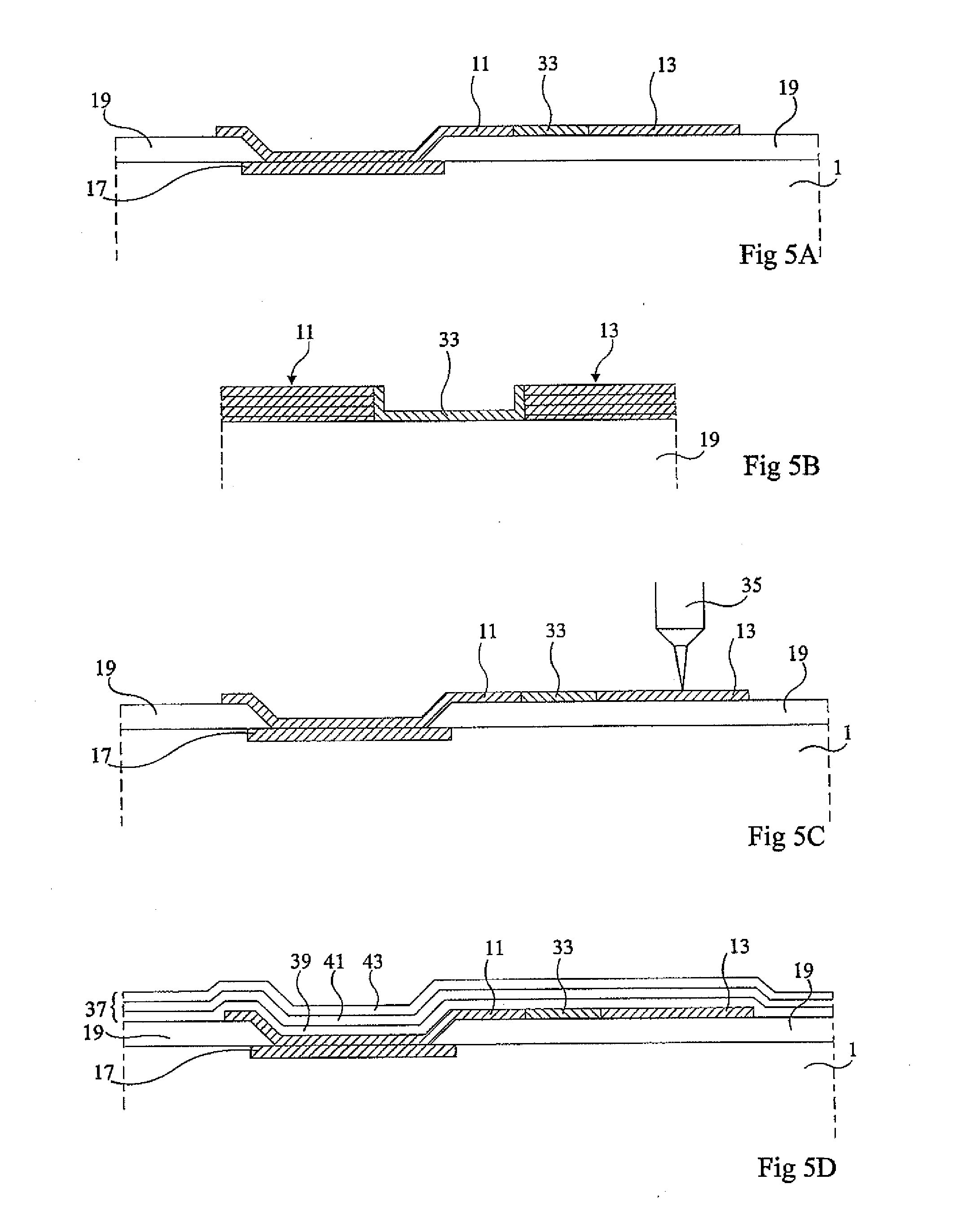
[0034]For clarity, the same elements have been designated with the same reference numerals in the different drawings and, further, as usual in the representation of integrated circuits, the various drawings are not to scale.

[0035]FIG. 1 is a cross-section view of an example of a connection between an integrated circuit chip and an encapsulation support.

[0036]Many connection elements 3 are formed on contact pads of an integrated circuit chip 1 of flip-chip type, that is, balls in the shown example. Chip 1 is attached to a support 5 via connection elements 3 which are positioned on contact pads of support 5. An encapsulation layer 7 which surrounds the different connection elements 3 is formed between integrated circuit chip 1 and support 5, which enables isolating these elements from one another and which also enables to avoid for humidity to reach connection elements 3.

[0037]FIG. 2 is a top view of an example of an integrated circuit chip such as that in FIG. 1, before flipping ther...


PUM


Abstract

A method for manufacturing and for testing an integrated circuit, including the steps of forming, on the upper portion of the integrated circuit, a passivation layer including openings at the level of metal tracks of the last interconnect stack of the integrated circuit; forming, in the openings, first pads connected to second pads formed on the passivation layer by conductive track sections, the first pads being intended for the connection of the integrated circuit; testing the integrated circuit by bringing test tips in contact with the second pads; and eliminating at least a portion of at least one of the conductive track sections.

Description

CROSS REFERENCE TO RELATED APPLICATIONS [0001]This application is a U.S. National Stage patent application based on PCT application number PCT / EP2009 / 056183, filed on May 20, 2009, entitled “Method For Manufacturing And Testing An Integrated Electronic Circuit”, which application claims the priority benefit of French patent application number 08 / 53069, filed on May 22, 2008, entitled “Method For Manufacturing And Testing An Integrated Electronic Circuit,” which applications are hereby incorporated by reference to the maximum extent allowable by law.BACKGROUND OF THE INVENTION [0002]1. Field of the Invention[0003]The present invention relates to a method for manufacturing and testing integrated circuits and, more specifically, to a method for testing integrated circuits directly on a semiconductor wafer and for preparing such integrated circuits for their encapsulation.[0004]2. Discussion of the Related Art[0005]Generally, integrated circuits formed on a semiconductor wafer are teste...

Claims


Application Information

Patent Timeline
IPC IPC(8): H01L21/66
CPCG01R1/0408H01L2224/05553G01R31/2884H01L22/32H01L24/10H01L24/11H01L24/12H01L2224/03H01L2224/0401H01L2224/13099H01L2224/16H01L2924/01002H01L2924/01013H01L2924/01014H01L2924/01022H01L2924/01028H01L2924/01029H01L2924/01033H01L2924/01046H01L2924/01047H01L2924/0105H01L2924/01058H01L2924/01073H01L2924/01074H01L2924/01079H01L2924/01082H01L2924/04941H01L2924/04953H01L2924/05042H01L2924/14H01L2924/15311H01L2924/30105H01L2924/30107H01L2224/0558H01L24/03H01L24/05H01L2224/05639H01L2224/05644H01L2924/01005H01L2924/01023H01L2924/01024G01R31/2822H01L24/13H01L2224/13111H01L2924/00014H01L2924/00H01L2224/0392H01L2224/13
Inventor COFFY, ROMAIN
Owner STMICROELECTRONICS (GRENOBLE 2) SAS
Why Eureka
Try Eureka