Memory device and fabrication process thereof

a technology of memory devices and fabrication processes, applied in semiconductor devices, digital storage, instruments, etc., can solve problems such as difficulty in satisfying all characteristics, and achieve the effect of reducing system cost and power consumption, and more freedom in memory design

Active Publication Date: 2011-04-28
SONY CORP
View PDF5 Cites 35 Cited by
  • Summary
  • Abstract
  • Description
  • Claims
  • Application Information

AI Technical Summary

Benefits of technology

[0011]Accordingly, there is a need for a memory device and a fabrication process thereof with which operating characteristics such as high-speed rewrite, and reliability characteristics such as data retention can be realized at the same time using a resistive-change memory element.
[0050]Further, the embodiments of the invention allow for selection of different combinations of the thickness and the material, and thus affords more freedom in memory design with regard to rewrite performance and data retention characteristic, making it possible to accommodate many variations.

Problems solved by technology

However, these characteristics often represent a trade-off, and it has been difficult to satisfy all characteristics at the same time.

Method used


Image

  • Memory device and fabrication process thereof
  • Memory device and fabrication process thereof
  • Memory device and fabrication process thereof

Examples


first embodiment

2. First Embodiment

[0130]Specific embodiments of the invention will now be described below.

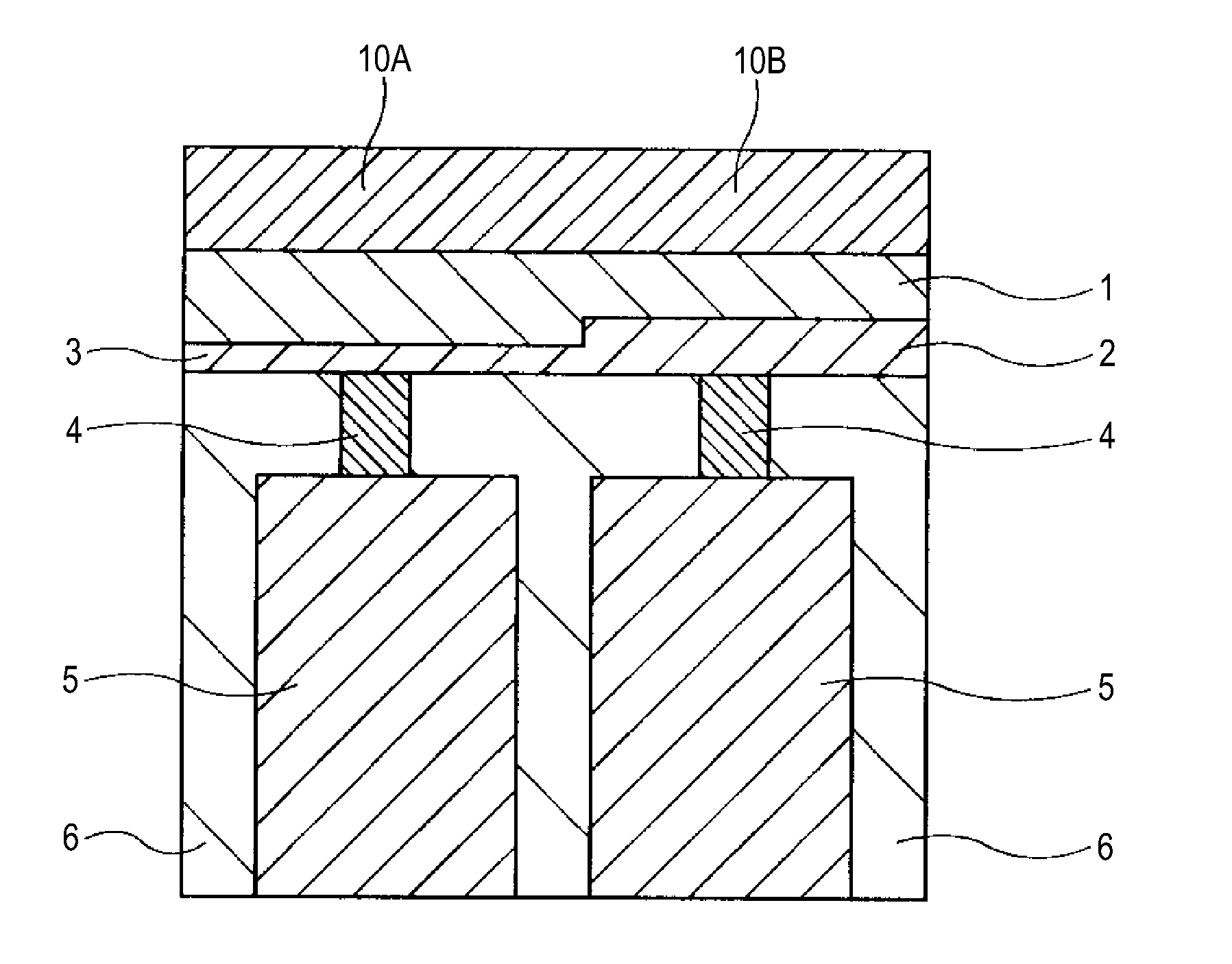
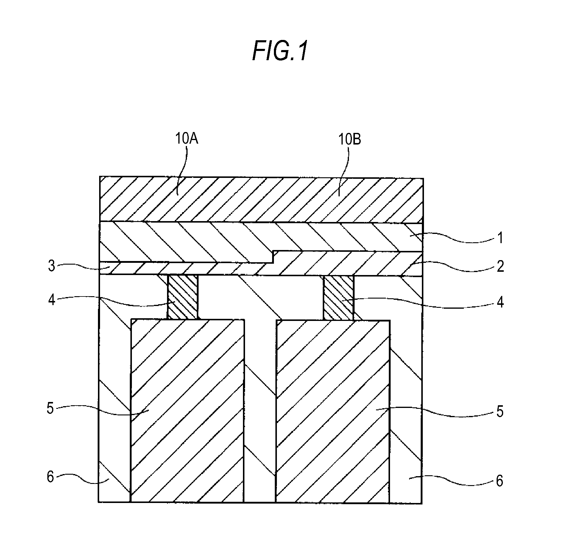
[0131]FIG. 1 shows an illustration of a schematic structure (cross sectional view of a relevant portion) of a memory device of First Embodiment of the invention.

[0132]The present embodiment is an application of the invention to a resistive-change memory element of the type in which, as described above, the resistive change operation is performed by the resistive-change layer and the resistive-change material supply layer (ion source layer).

[0133]The memory device is configured using resistive-change memory elements. The cross section illustrated in FIG. 1 shows an adjacent portion of two memory elements of different characteristics.

[0134]Each of these two memory elements is configured to include a resistive-change material supply layer 1, a resistive-change layer 2 or 3, a plug electrode (electrode layer) 4, and a lower electrode 5. The plug electrode (electrode layer) 4 and the lower electrod...

second embodiment

3. Second Embodiment

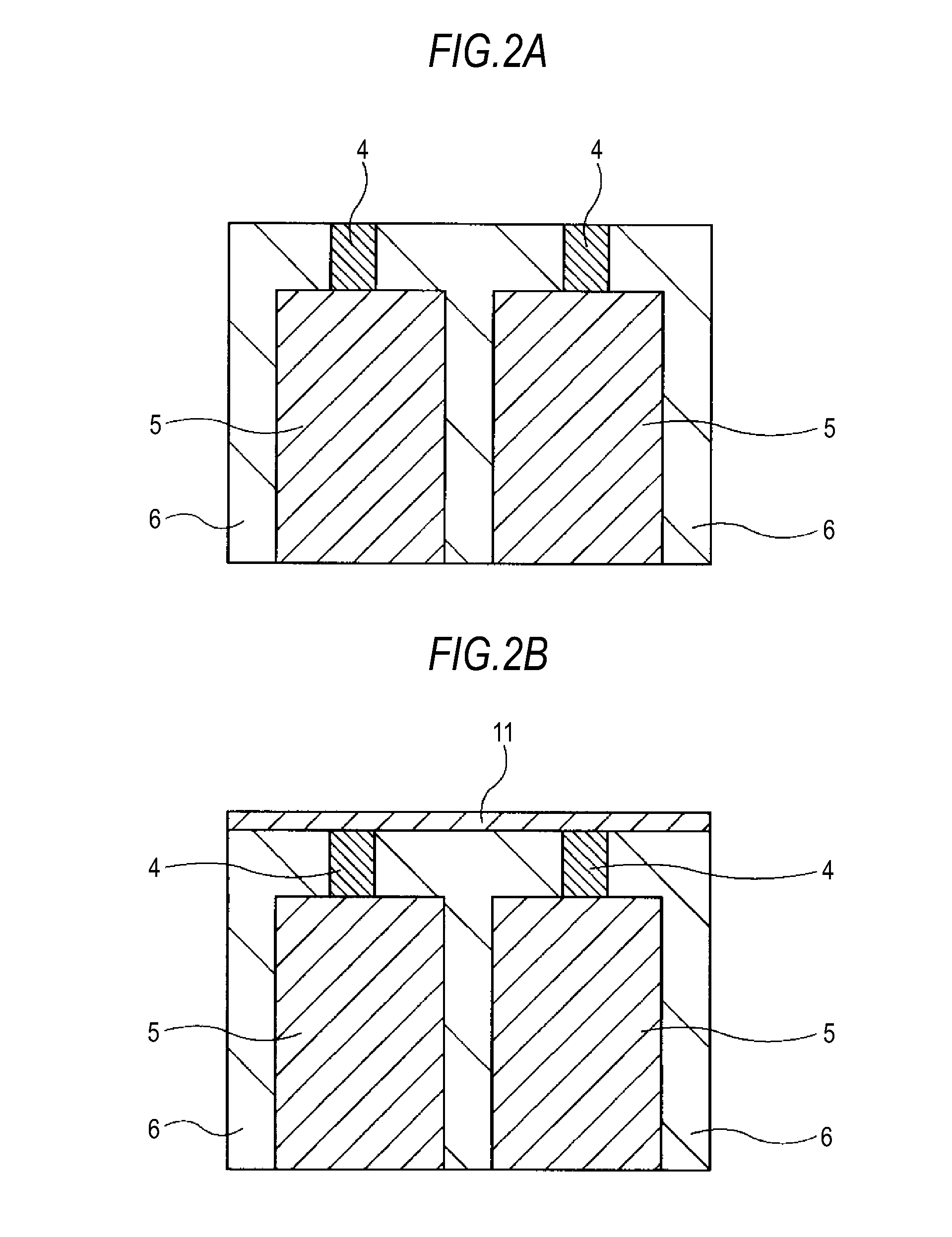
[0161]FIG. 5 shows an illustration of a schematic structure (cross sectional view of a relevant portion) of a memory device of Second Embodiment of the invention.

[0162]The cross section illustrated in FIG. 5 shows an adjacent portion of two memory elements of different characteristics.

[0163]The basic configuration of the two memory elements is the same as that described in First Embodiment.

[0164]In the memory device of the present embodiment, the thicknesses and the materials of the resistive-change layers 2 and 3 are different for the two memory elements illustrated in FIG. 5. Specifically, the memory device has the combination of the configurations described in (1) and (2) above.

[0165]In the left memory element (first memory element) of FIG. 5, only the first resistive-change material layer 11 forms the first resistive-change layer 3. In the right memory element (second memory element), the laminate of a second resistive-change material layer 13 and the first r...

third embodiment

4. Third Embodiment

[0174]FIG. 6 shows an illustration of a schematic structure (cross sectional view of a relevant portion) of a memory device of Third Embodiment of the invention.

[0175]The cross section illustrated in FIG. 6 shows an adjacent portion of two memory elements of different characteristics.

[0176]The basic configuration of the two memory elements is the same as that described in the foregoing embodiments.

[0177]In the memory device of the present embodiment, the resistive-change layers 2 and 3 have the same thickness but different materials for the two memory elements illustrated in FIG. 6. Specifically, the memory device has the configuration described in (2) above.

[0178]In the left memory element (first memory element) in FIG. 6, only the first resistive-change material layer 11 forms the first resistive-change layer 3. In the right memory element (second memory element), a third resistive-change material layer 14 forms the second resistive-change layer 2.

[0179]The mate...


PUM


Abstract

A memory device that includes a resistive-change memory element, the memory device includes: a first memory element that includes a first resistive-change layer and a first electrode connected to the first resistive-change layer; and a second memory element that includes a second resistive-change layer and a second electrode connected to the second resistive-change layer, wherein at least one of the thickness and the material of the second resistive-change layer and the area of the second electrode in contact with the second resistive-change layer is different from the corresponding one of the thickness and the material of the first resistive-change layer and the area of the first electrode in contact with the first resistive-change layer.

Description

BACKGROUND OF THE INVENTION[0001]1. Field of the Invention[0002]The present invention relates to memory devices that use resistive-change memory elements, and fabrication processes of such memory devices.[0003]2. Description of the Related Art[0004]Semiconductor devices that include nonvolatile memory such as EEPROM (Electrically Erasable and Programmable ROM) and flash memory have been commonly used in a wide range of fields.[0005]Improving reliability such as rewrite count and data retention durability, and miniaturization of the memory structure pose significant challenges to the nonvolatile memory.[0006]Resistive-change nonvolatile memory has gained attention as having advantages in reliability and miniaturization over the structure of the currently marketed flash memory as represented by the floating-type structure.[0007]Regarding such resistive-change nonvolatile memory, for example, ReRAM (Resistive Random Access Memory) and PCRAM (Phase Change Random Access Memory) have been...

Claims


Application Information

Patent Timeline
Patent Type & Authority Applications(United States)
IPC IPC(8): H01L45/00H01L21/02
CPCG11C13/0002H01L45/145H01L45/141H01L45/1608H01L27/2472H01L45/1233H01L45/1266H01L45/146H01L45/165H01L45/085H10B63/82H10N70/245H10N70/8416H10N70/883H10N70/021H10N70/043H10N70/061H10N70/8833H10N70/826H10N70/882
Inventor SUMINO, JUNYASUDA, SHUICHIRO
Owner SONY CORP
Why Eureka
Try Eureka