Low-resistance interconnects and methods of making same

a technology of low-resistance interconnects and methods, applied in the direction of semiconductor devices, semiconductor/solid-state device details, electrical apparatus, etc., can solve the problems of increased heat and increased likelihood of device failur

Active Publication Date: 2011-04-28
MICRON TECH INC
View PDF51 Cites 6 Cited by
  • Summary
  • Abstract
  • Description
  • Claims
  • Application Information

AI Technical Summary

Problems solved by technology

One drawback of narrower vertical interconnects, however, is that the smaller cross-sectional area of the conductive material in the interconnect may increase the electrical resistance of the interconnect, resulting in increased heat and a greater likelihood of device failure.

Method used


Image

  • Low-resistance interconnects and methods of making same
  • Low-resistance interconnects and methods of making same
  • Low-resistance interconnects and methods of making same

Examples


Embodiment Construction

[0010]One or more specific embodiments of the present invention will be described below. In an effort to provide a concise description of these embodiments, not all features of an actual implementation are described in the specification. It should be appreciated that in the development of any such actual implementation, as in any engineering or design project, numerous implementation-specific decisions must be made to achieve the developers' specific goals, such as compliance with system-related and business-related constraints, which may vary from one implementation to another. Moreover, it should be appreciated that such a development effort might be complex and time consuming but would nevertheless be a routine undertaking of design, fabrication, and manufacture for those of ordinary skill having the benefit of this disclosure.

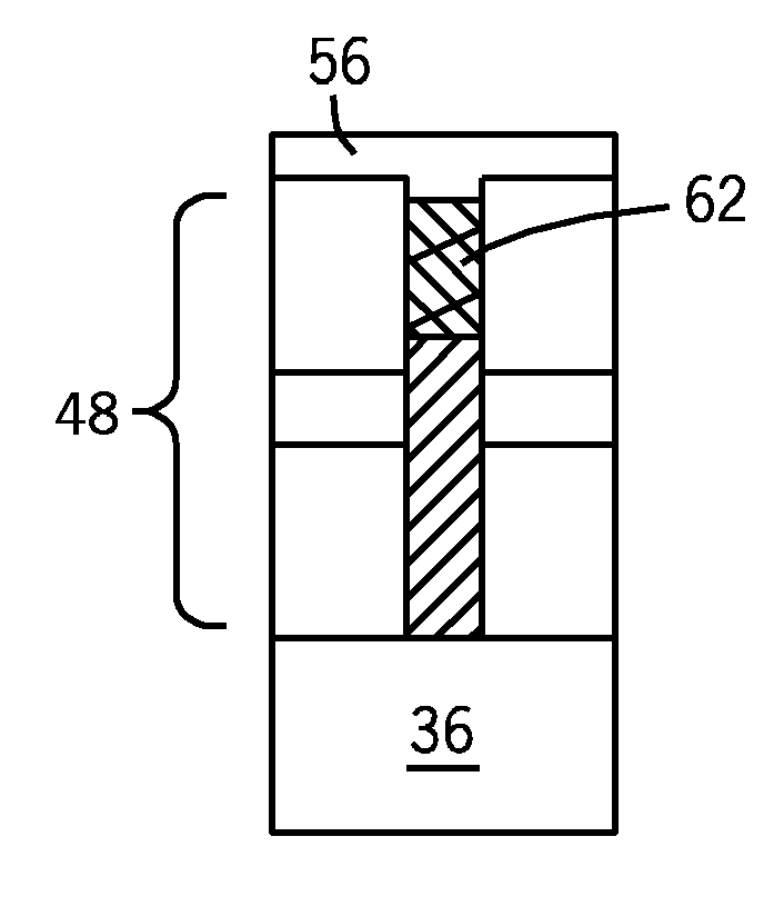
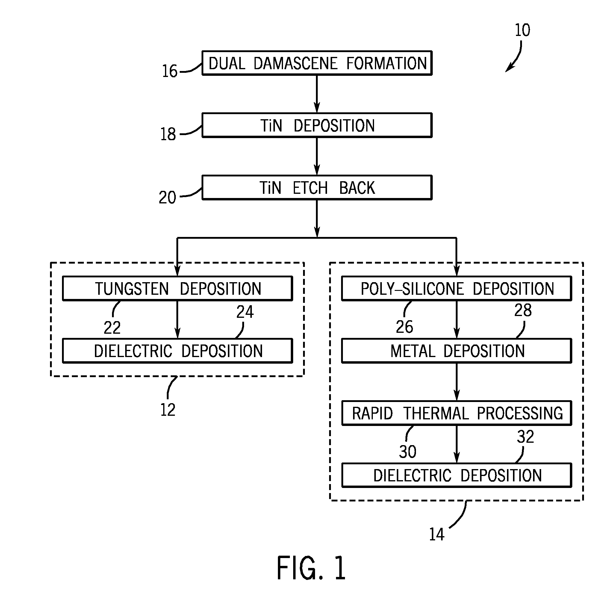
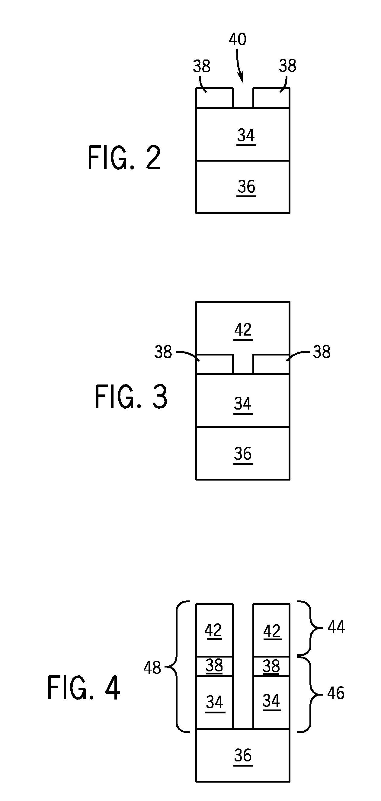
[0011]Embodiments of the present invention generally relate to methods for fabricating a low-resistance interconnect. Some embodiments of the present inven...


PUM

PropertyMeasurementUnit
widthaaaaaaaaaa
widthaaaaaaaaaa
widthaaaaaaaaaa

Abstract

Devices and methods for providing low-resistance interconnects in a semiconductor device are provided. Specifically, one or more embodiments of the present invention relate to disposing a conductive material in a trench without disposing a resistive barrier material between the conductive material and the sidewalls of the trench so that the conductive material takes up the full width of the trench. For example, the trench may be disposed over one or more contacts made of a barrier material such as titanium nitride that also acts as a seed, and the conductive material may be grown on top of the titanium nitride to fill the trench.

Description

CROSS-REFERENCE TO RELATED APPLICATION[0001]This application is a divisional of U.S. patent application Ser. No. 12 / 119,994, which was filed on May 13, 2008.BACKGROUND[0002]1. Field of the Invention[0003]Embodiments of the present invention relate generally to the field of semiconductor devices. More particularly, embodiments of the present invention relate to improved semiconductor devices and improved fabrication techniques for semiconductor devices.[0004]2. Description of the Related Art[0005]As electronics continue toward greater miniaturization and faster processing speeds, various techniques have been developed for more compact packaging and increased transmission speeds in semiconductor chips. For example, one trend has been the stacking of circuit components in multiple layers on a chip. This allows more components to be fabricated in a given area and also reduces the lengths of the vertical interconnects, the conductive lines that electrically couple the circuit components ...

Claims


Application Information

Patent Timeline
Patent Type & Authority Applications(United States)
IPC IPC(8): H01L23/52
CPCH01L21/7681H01L21/76843H01L21/76876H01L21/76877H01L23/5226H01L2924/0002H01L23/53295H01L2924/00H01L21/76807H01L23/528H01L23/53266H01L23/53271H01L23/535
Inventor GOSWAMI, JAYDEBMCTEER, ALLEN
Owner MICRON TECH INC
Why Eureka
Try Eureka