Nonvolatile memory device and method for fabricating the same

a memory device and non-volatile technology, applied in the direction of semiconductor devices, basic electric elements, electrical equipment, etc., can solve the problem of high equipment requirements for the miniaturization of patterns, and achieve the effect of reducing the resistance of the source/drain region and increasing the curren

Inactive Publication Date: 2011-05-05
SAMSUNG ELECTRONICS CO LTD
View PDF8 Cites 34 Cited by
  • Summary
  • Abstract
  • Description
  • Claims
  • Application Information

AI Technical Summary

Benefits of technology

[0010]It is therefore a separate feature of an embodiment to provide a nonvolatile memory device and a method for fabricating such a memory device in which the resistance of the source / drain region may be reduced in the memory cells relative to comparable conventional devices. Thus, a current can be increased in the memory cells storing data.

Problems solved by technology

Further, miniaturization of patterns requires highly expensive equipment.
The degree of integration of two-dimensional semiconductor memory devices is being steadily increased, but there are limits.

Method used


Image

  • Nonvolatile memory device and method for fabricating the same
  • Nonvolatile memory device and method for fabricating the same
  • Nonvolatile memory device and method for fabricating the same

Examples


Embodiment Construction

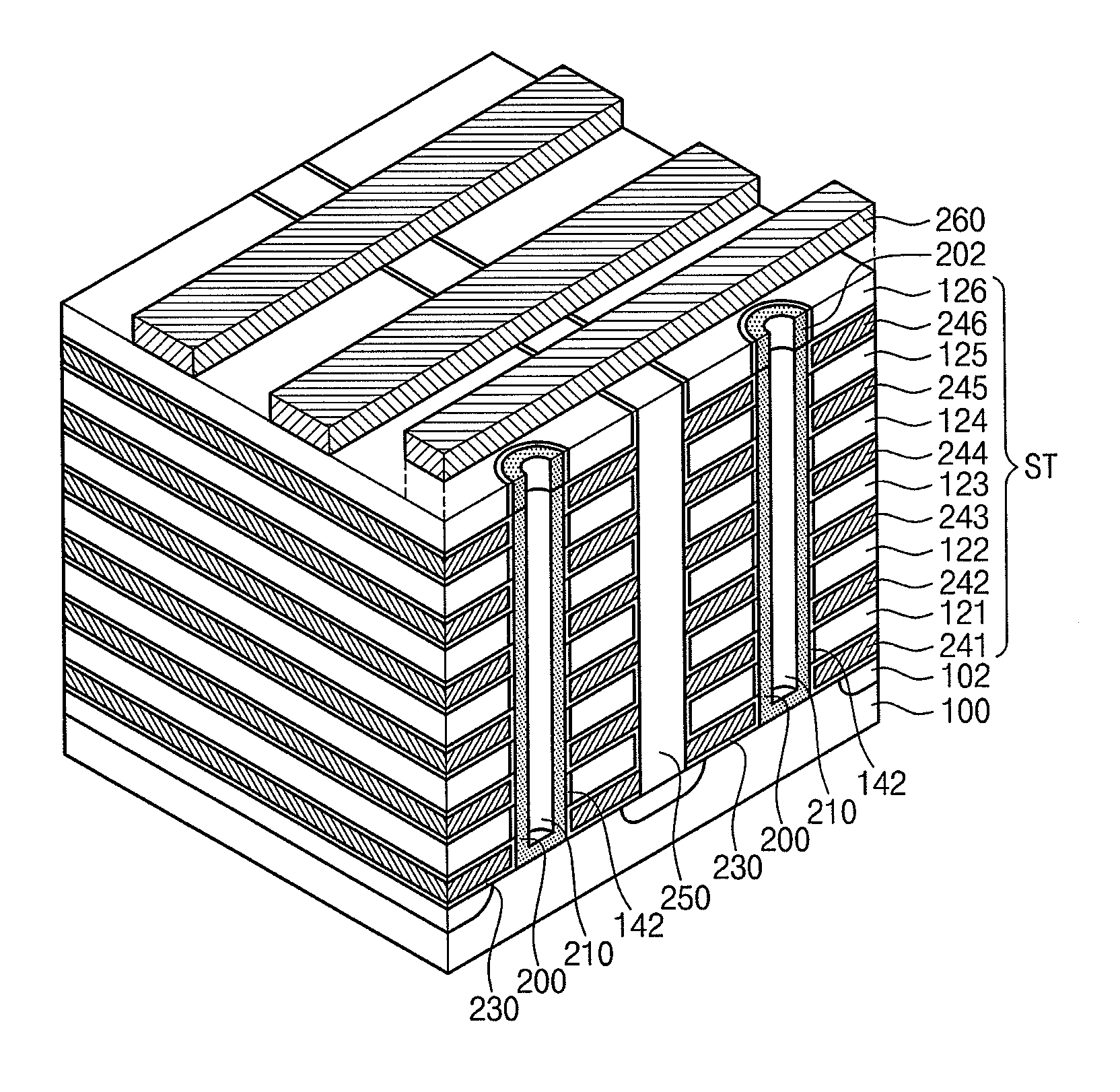
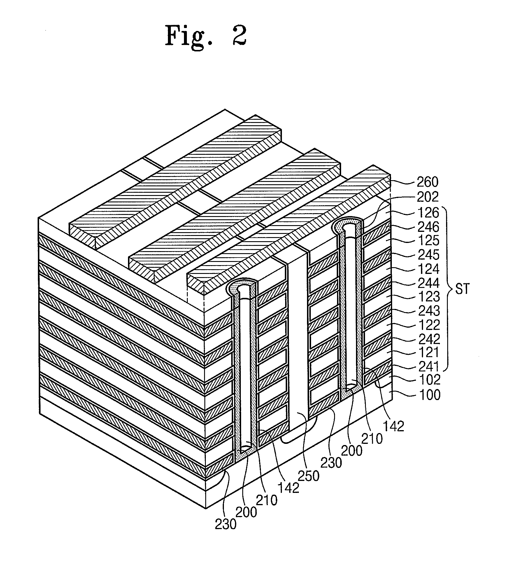
[0041]Korean Patent Application No. 10-2009-0093292, filed on Sep. 30, 2009, in the Korean Intellectual Property Office, and entitled: “Nonvolatile Memory Device and Method for Fabricating the Same,” is incorporated by reference herein in its e

[0042]Exemplary embodiments of the inventive concept will be described below in more detail with reference to the accompanying drawings. The inventive concept may, however, be embodied in different forms and should not be construed as limited to the embodiments set forth herein. Rather, these embodiments are provided so that this disclosure will be thorough and complete, and will fully convey the scope of the inventive concept to those skilled in the art.

[0043]In the drawings, the dimensions of layers and regions may be exaggerated for clarity of illustration. It will be understood that when an element such as a layer, film, region, or substrate is referred to as being “on” another element, it can be directly on the other element or intervenin...


PUM


Abstract

Provided are a nonvolatile memory device and a method for fabricating the same. The nonvolatile memory device may include a stacked structure, a semiconductor pattern, an information storage layer, and a fixed charge layer. The stacked structure may be disposed over a semiconductor substrate. The stacked structure may include conductive patterns and interlayer dielectric patterns alternately stacked therein. The semiconductor pattern may be connected to the semiconductor substrate by passing through the stacked structure. The information storage layer may be disposed between the semiconductor pattern and the conductive patterns. The fixed charge layer may be disposed between the semiconductor pattern and the interlayer dielectric pattern. The fixed charge layer may include fixed charges. Electrical polarity of the fixed charges may be equal to electrical polarity of majority carriers of the semiconductor pattern.

Description

BACKGROUND[0001]1. Field[0002]The present disclosure herein relates to a nonvolatile memory device and a method for fabricating the same, and more particularly, to a nonvolatile memory device having a three-dimensional structure and a method for fabricating the same.[0003]2. Description of the Related Art[0004]The degree of integration of semiconductor devices needs to be increased to meet consumer demands for excellent performance and low prices. In semiconductor memory devices, since the degree of integration is an important factor affecting the price of products, increasing the degree of integration is of particular importance. In typical two dimensional or planar semiconductor devices, since the degree of integration is mainly determined by the area occupied by a unit memory cell, the degree of integration is greatly affected by the level of technologies of forming a micro pattern. Further, miniaturization of patterns requires highly expensive equipment. The degree of integratio...

Claims


Application Information

Patent Timeline
Patent Type & Authority Applications(United States)
IPC IPC(8): H01L29/792
CPCH01L27/11551H01L27/11556H01L27/11578H01L29/7926H01L29/66833H01L29/7883H01L29/792H01L29/66825H10B41/20H10B43/20H10B41/27
Inventor HUO, ZONGLIANGLEE, MYOUNGBUMHWANG, KIHYUNSHIN, SEUNGMOKKIM, SUNJUNG
Owner SAMSUNG ELECTRONICS CO LTD
Why Eureka
Try Eureka