

Electrostatic protection device
- Summary
- Abstract
- Description
- Claims
- Application Information
AI Technical Summary
Benefits of technology
Problems solved by technology
Method used
Image

Examples
Embodiment Construction
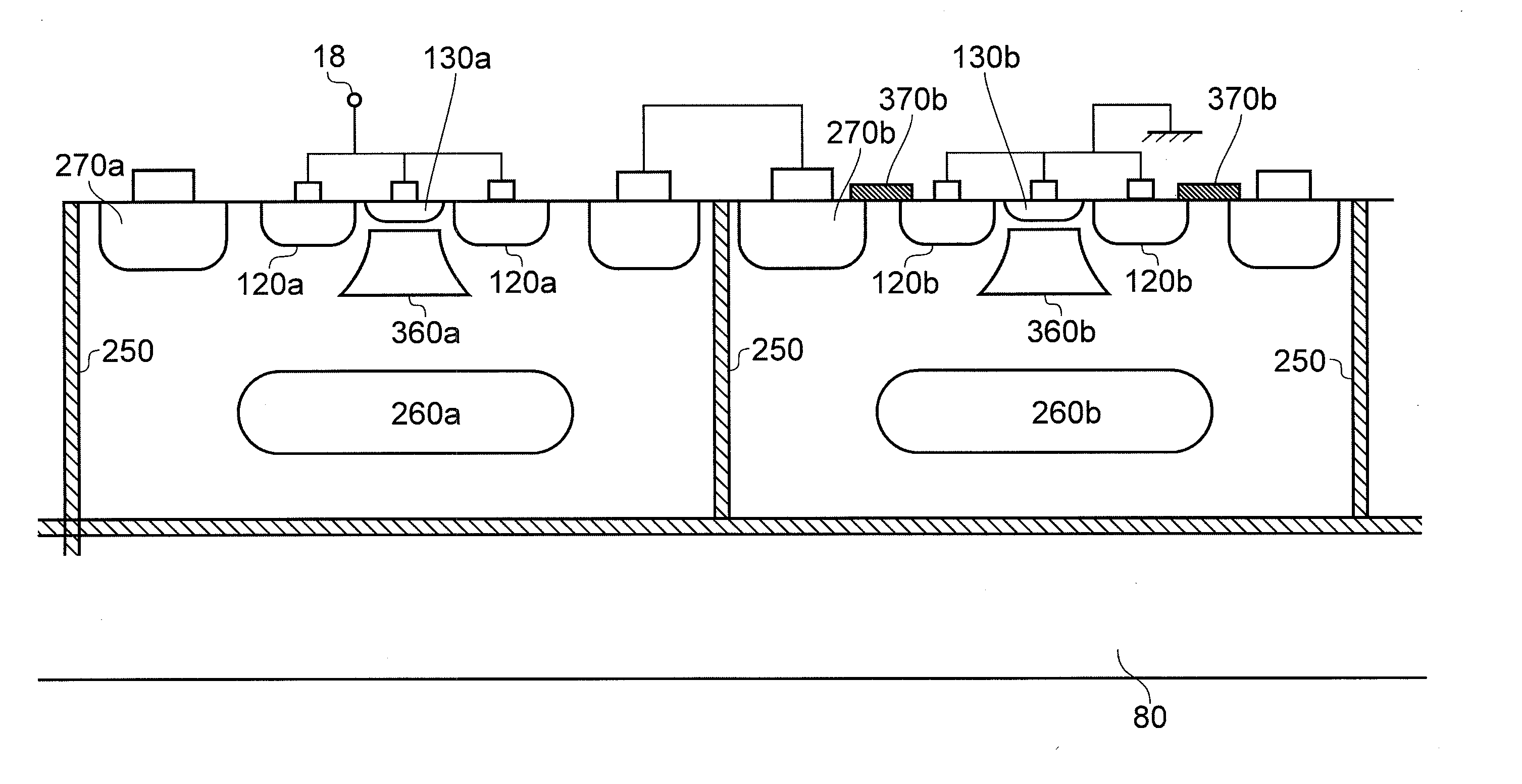
[0026]Terms such as above, below, over, and so on as used herein refer to a semiconductor device orientated as shown in the figures and should be construed accordingly. It should also be appreciated that, because regions within a semiconductor device are defined by doping different parts of a semiconductor with differing impurities or differing concentrations of impurities, discrete physical boundaries between different regions may not actually exist in the completed device but instead regions may transition form one to another. Some boundaries as shown in the accompanying figures are of this type and are illustrated as abrupt structures merely for the assistance of the reader. The skilled artisan can readily determine with such gradients where to set boundaries for discrete functional diffusion regions in a semiconductor device.
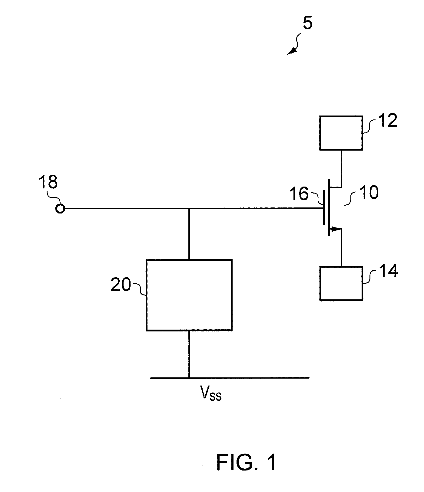
[0027]As noted before, transistors have sometimes been used to provide electrostatic protection devices. However an integrated circuit may contain millions ...
PUM
 Abstract
Description
Claims
Application Information