High-k/metal gate CMOS finfet with improved pfet threshold voltage

a technology of metal gate and cmos fin, which is applied in the direction of semiconductor devices, basic electric elements, electrical apparatus, etc., can solve the problems of degrading the electrostatics of the fin, increasing the total fin width, and achieving a final width of 20 nm, which is unacceptable for 22 nm nodes and beyond

Active Publication Date: 2011-05-12
GLOBALFOUNDRIES US INC
View PDF0 Cites 154 Cited by
  • Summary
  • Abstract
  • Description
  • Claims
  • Application Information

AI Technical Summary

Problems solved by technology

However, when a layer is grown on finFET sidewalls, the total fin width increases, degrading electrostatics of the finFET.
For example, even 5 nm of growth on each side of a 10 nm fin results in the final width of 20 nm which is unacceptable for 22 nm nodes and beyond.

Method used


Image

  • High-k/metal gate CMOS finfet with improved pfet threshold voltage
  • High-k/metal gate CMOS finfet with improved pfet threshold voltage
  • High-k/metal gate CMOS finfet with improved pfet threshold voltage

Examples


Embodiment Construction

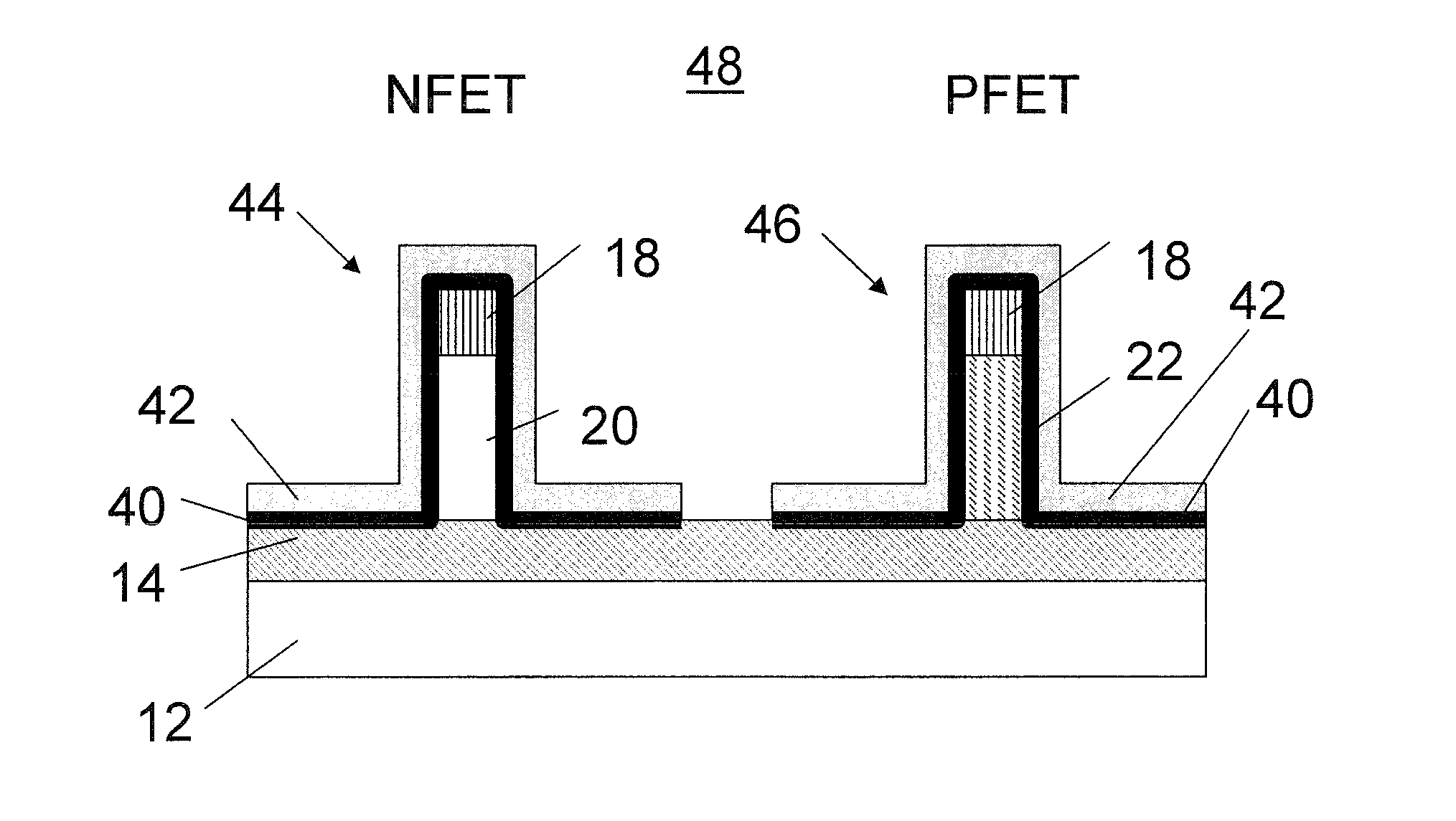
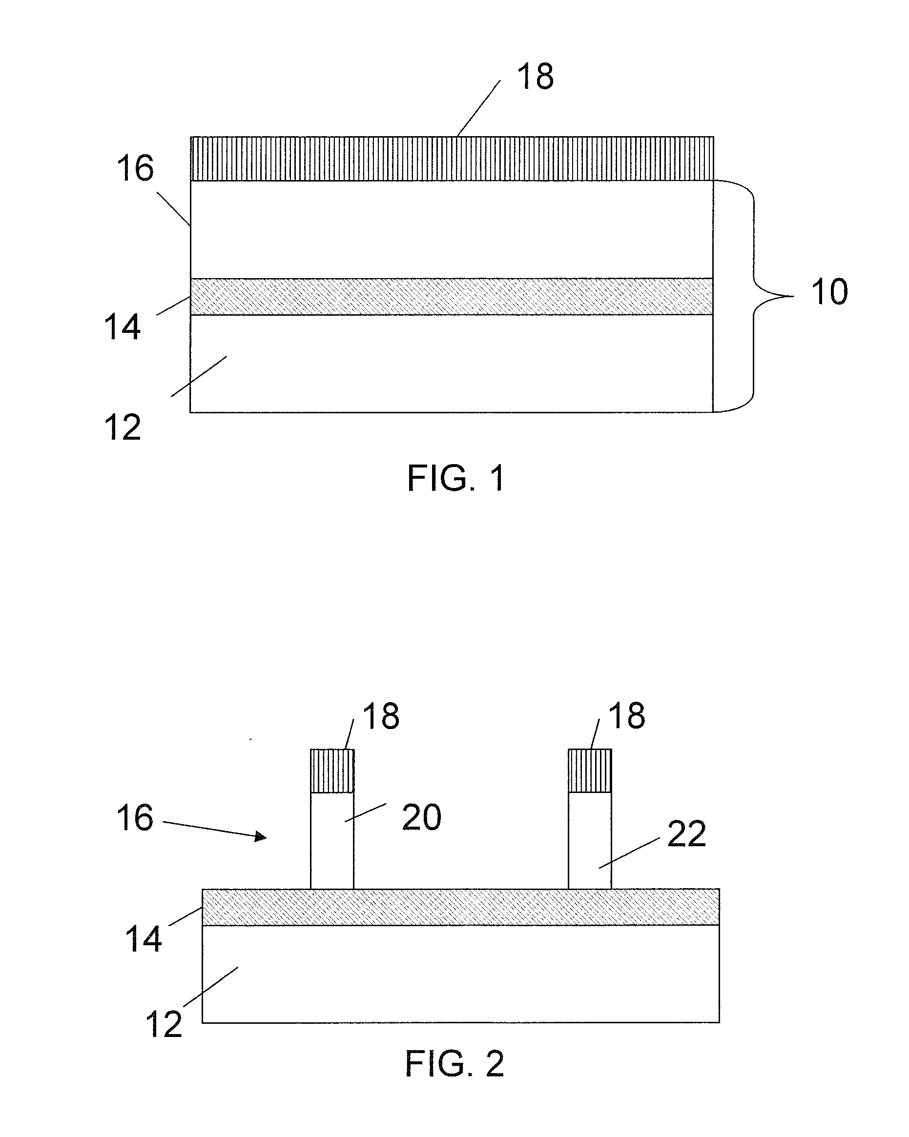
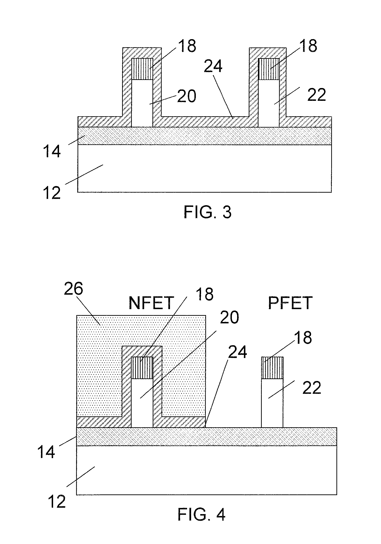
[0020]In accordance with the present principles, methods and structures for forming a high dielectric constant (high-k)-metal gate fin field effect transistor (FET) complementary metal oxide semiconductor (CMOS) device is disclosed. The device and method provide a p-type field effect transistor (pFET) within a target threshold voltage. An n-type field effect transistor (nFET) is formed on a fin made from a substrate material. A corresponding pFET is formed on a fin which is processed by pushing or diffusing an element into the substrate material to form a new structure. In one example, the substrate includes silicon which is employed to form the fin for the nFET. In this example, a fin for the pFET includes silicon as well, but Germanium (Ge) is pushed into silicon to form a SiGe fin for the formation of the pFET. The pFET is formed by, e.g., oxidation condensation (to push Ge into a Si fin during oxidation).

[0021]In this way, the pFET finFET with a SiGe body achieves a corrected th...


PUM


Abstract

A device and method for fabrication of fin devices for an integrated circuit includes forming fin structures in a semiconductor material of a semiconductor device wherein the semiconductor material is exposed on sidewalls of the fin structures. A donor material is epitaxially deposited on the exposed sidewalls of the fin structures. A condensation process is applied to move the donor material through the sidewalls into the semiconductor material such that accommodation of the donor material causes a strain in the semiconductor material of the fin structures. The donor material is removed, and a field effect transistor is formed from the fin structure.

Description

BACKGROUND[0001]1. Technical Field[0002]The present invention relates to semiconductor fabrication and more particularly to high k / metal gate devices and methods for fabricating the same having tuned p-type field effect transistors.[0003]2. Description of the Related Art[0004]In conventional high dielectric constant (high-K) metal gate (HK / MG) fin field effect transistors (FET), a p-type FET (pFET) usually exhibits a threshold voltage (Vt) that is higher than a target value. Forming a thin layer in a channel may be effective to lower planar pFET Vt. However, when a layer is grown on finFET sidewalls, the total fin width increases, degrading electrostatics of the finFET. For example, even 5 nm of growth on each side of a 10 nm fin results in the final width of 20 nm which is unacceptable for 22 nm nodes and beyond. Therefore, there is a need for tuning pMOS finFET without compromising device performance.SUMMARY[0005]A device and method for fabrication of fin devices for an integrated...

Claims


Application Information

Patent Timeline
Patent Type & Authority Applications(United States)
IPC IPC(8): H01L29/49H01L21/84
CPCH01L21/845H01L29/66795H01L29/1054H01L27/1211
Inventor BASKER, VEERARAGHAVAN S.CHENG, KANGGUODORIS, BRUCE B.FALTERMEIER, JOHNATHAN E.KHAKIFIROOZ, ALI
Owner GLOBALFOUNDRIES US INC
Why Eureka
Try Eureka