Optical element for a light emitting device and a method of manufacturing thereof

a technology of optical elements and light emitting devices, which is applied in the direction of packaging, light sources, electrical devices, etc., can solve the problems of degrading the function of the optical element, unfavorable deviations from the regular light intensity distribution, etc., and achieves the effect of high durability

Active Publication Date: 2011-05-19
KONINKLIJKE PHILIPS ELECTRONICS NV
View PDF2 Cites 20 Cited by
  • Summary
  • Abstract
  • Description
  • Claims
  • Application Information

AI Technical Summary

Benefits of technology

[0013]It is also an object of the present invention to provide a manufacturing method of an optical element comprising a sintered ceramic body, wherein high physical contact between the wavelength converting layer and the scattering layer is provided, i.e. without the use of adhesives. Further, it is an object to provide a manufacturing method in which the two layers of the optical element are produced in the same manufacturing step. Furthermore, a robust material structure with high durability, a high manufacturing performance, and an easy and a cost-effective way of producing optical elements is desired.
[0032]In a fourth aspect, the present invention provides a method for manufacturing a light emitting device comprising at least one LED, comprising: providing an optical element according to any of the product claims or obtainable by any of the method claims; and arranging the optical element to receive at least part of the light emitted by the light emitting diode, and such that the first layer faces at least one LED. By using the optical element according to the invention in the manufacturing of a light emitting device, a light emitting device with high durability is provided.

Problems solved by technology

There are several issues that have to be considered when optical elements comprise both a wavelength converting layer and a scattering layer.
The optical element is exposed to temperature variations during use, which may result in heat-induced stresses caused by the use of materials with different thermal expansion properties in the wavelength converting layer and the scattering layer.
This may result in undesired deviations from the regular light intensity distribution.
In addition, chemical interactions between the wavelength converting layer and the scattering layer may result in degraded function of the optical element, such as destroyed luminescence or a change of the emission color.

Method used


Image

  • Optical element for a light emitting device and a method of manufacturing thereof
  • Optical element for a light emitting device and a method of manufacturing thereof

Examples


example 1

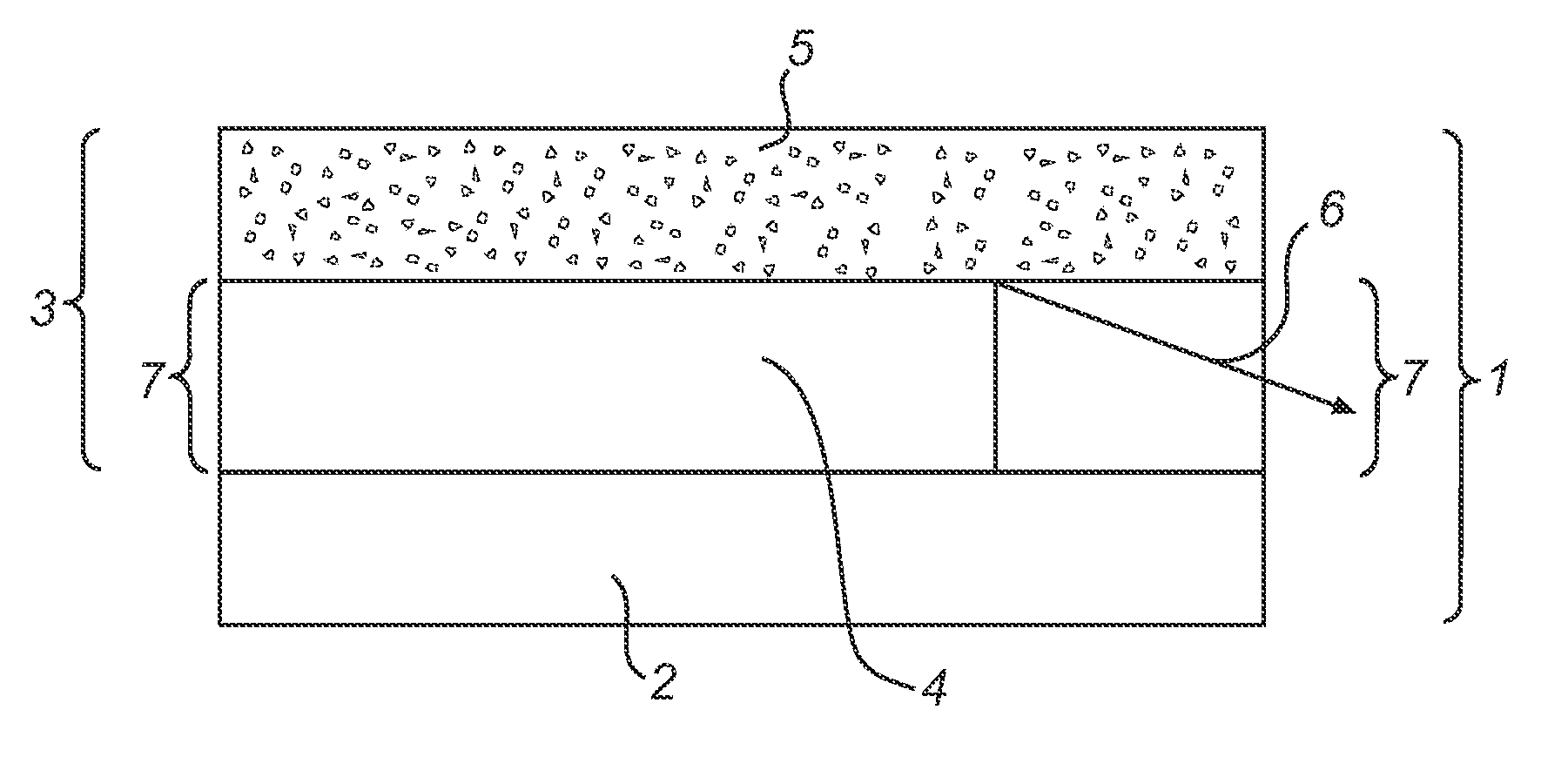
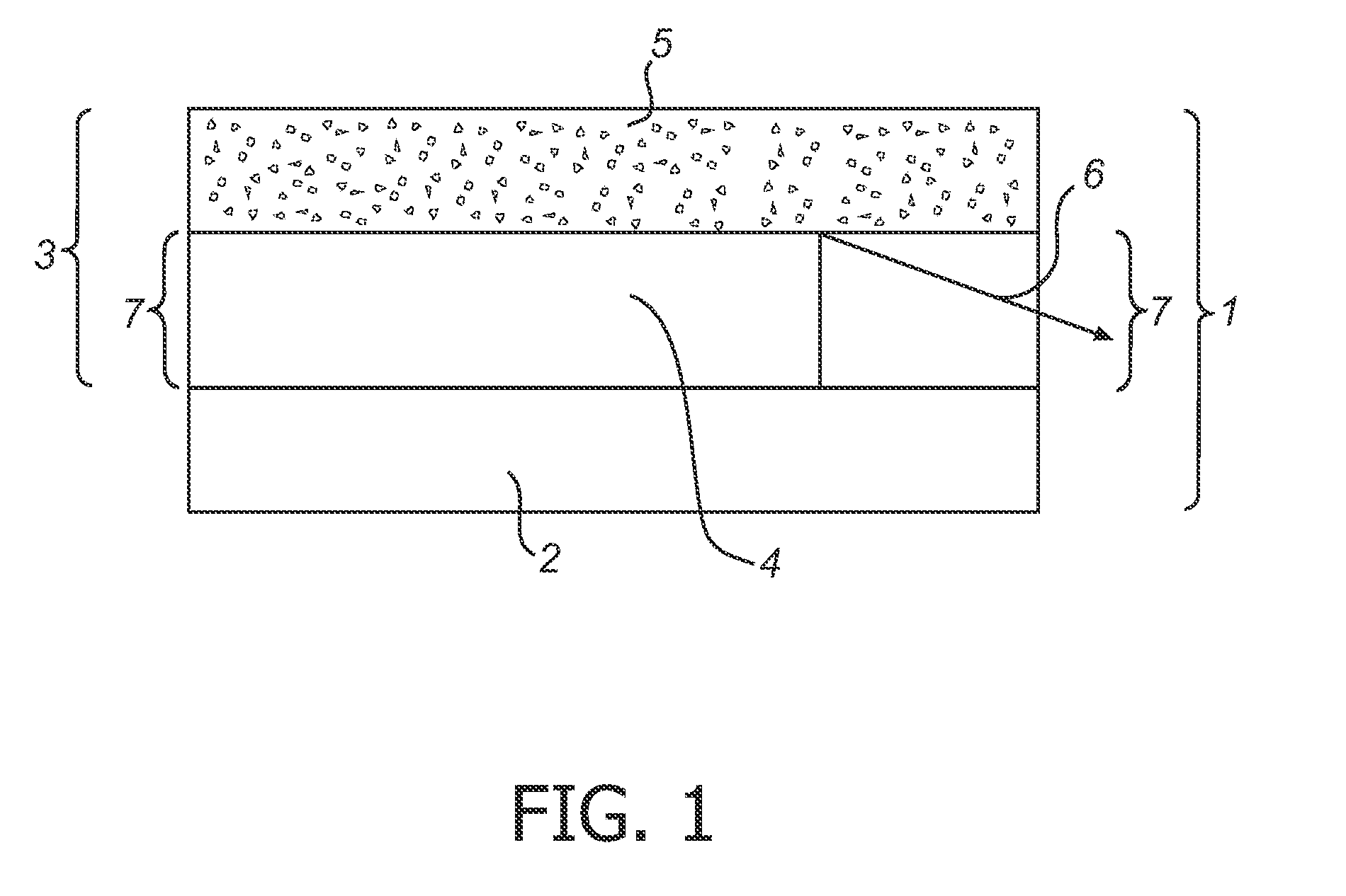
[0053]Preparation of an optical element according to the invention comprising a first layer, wavelength converting layer, and a second layer with scattering properties, wherein the optical element is based on Y3Al5O12.

[0054]The following oxide constituents were used for the green bodies:

[0055]Y2O3, specific area 15 m2 / g, obtainable from Rodia;

[0056]Al2O3, specific area 8 m2 / g, obtainable from Reynolds / Malakoff;

[0057]CeO2, specific area 4 m2 / g, obtainable from Rodia; and

[0058]Gd2O3 (in case of red-shifted wavelength converting layer), specific area 17 m2 / g.

[0059]In addition, SiO2, which is a suitable fluxing agent for sintering of Y3Al5O12 based ceramic materials was added to the first layer in a concentration of 200-2000 ppm and to the second layer in a concentration of 0-500 ppm. The first layer was doped with 0.01-2% Ce.

[0060]The green bodies were prepared by uniaxial pressing of the two powder-layers (layer 4 and 5 in FIG. 1) in one go, followed by cold-isostatic-pressing for max...


PUM

PropertyMeasurementUnit
reflectivityaaaaaaaaaa
diameteraaaaaaaaaa
porosityaaaaaaaaaa

Abstract

The present invention relates to an optical element for a light emitting device, wherein the optical element comprises a sintered ceramic body (3) comprising a wavelength converting layer (4) and a scattering layer (5), and to a method of manufacturing thereof. More specifically, the invention relates to an optical element, comprising a sintered ceramic body (3) of a first layer (4) and a second layer (5) arranged on the first layer, wherein the first layer comprises a wavelength converting material, the porosity of the second layer is higher than the porosity of the first layer, and pores in the second layer are arranged to provide scattering of a light beam. The method for manufacturing of the optical element comprises providing a green body comprising a first layer of a first material and a second layer of a second material; and co-sintering said layers into a sintered ceramic body; the compositions of the first and second layer are adapted such that after sintering, the porosity of the second layer is higher than the porosity of the first layer, and pores in said second layer are arranged to provide scattering of a light beam.

Description

FIELD OF THE INVENTION[0001]The present invention relates to an optical element for a light emitting device, wherein the optical element comprises a sintered ceramic body comprising a wavelength converting layer and a scattering layer, and to a method of manufacturing thereof.BACKGROUND OF THE INVENTION[0002]Light emitting devices comprise at least one light emitting diode (LED) which generally is arranged with an optical element. The optical element generally comprises a wavelength converting layer comprising a phosphor and / or a layer that redirects the emitted light. Thereby, the primary light emitted from the LED can be influenced in various ways.[0003]A top-emitting LED refers to a light emitting diode having an optical element, wherein the light generated by the LED is illuminated at the top surface of the optical element. For optical elements in top-emitting LEDs, properties such a high transparency and optimal wavelength conversion are desired. This is preferably achieved by ...

Claims


Application Information

Patent Timeline
Patent Type & Authority Applications(United States)
IPC IPC(8): F21V11/00B32B3/26B32B37/06B32B37/00
CPCB32B18/00Y10T156/10C04B2235/3224C04B2235/3225C04B2235/3229C04B2235/3418C04B2235/5409C04B2235/604C04B2235/6562C04B2235/6565C04B2235/77C04B2237/343C04B2237/586C04B2237/704C09K11/7774H01L33/44H01L33/507C04B35/44H01L33/505H01L2933/0091Y10T428/249969H01L33/50
Inventor CILLESSEN, JOHANNES FRANCISCUS MARIAVAN HAL, HENRICUS ALBERTUS MARIAJAGT, HENDRIK JOHANNES BOUDEWIJNSTEIGELMANN, OLIVER JENS
Owner KONINKLIJKE PHILIPS ELECTRONICS NV
Why Eureka
Try Eureka