Serviceable conformal em shield

a conformal shield and shielding technology, applied in the field of electromagnetic and radiofrequency shielding solutions, can solve the problems of affecting affecting the safety of the system, so as to reduce the overall size of the component, and reduce the effect of em leakag

Inactive Publication Date: 2011-05-26
LOCKHEED MARTIN CORP
View PDF39 Cites 36 Cited by
  • Summary
  • Abstract
  • Description
  • Claims
  • Application Information

AI Technical Summary

Benefits of technology

[0009]Variations of a deposition process for an insulating layer may include spraying, dispensing, powder-coating, laminating, painting, vapor deposition, flame spray, or submerging the component(s) in a desired electrically insulating material such as elastomer, silicone, latex, ceramic, glass, or other suitable passivating material which may allow for easy removal of the coating. Variations of a passivation layer may include directly written silicone or sprayed-on urethane. Further variations of a passivation layer may include acrylic, parylene, kraton, noryl, etc. In some cases, a urethane layer may provide improved adhesion between the passivating layer and its substrate.
[0017]Advantages of variations of EM shielding coatings as discussed above may include reduction of weight, bulk, space or volume requirements, and cost for shielded components. This reduces the overall size of the component and is pertinent to any weight or size sensitive application, such as aviation-related and space-related applications, as well as the continual miniaturization of consumer electronics devices. Further advantages may include reduced EM leakage in variations having shielding on all of a component except for actual connection points or having EM shielding arranged such that it blocks transmission paths.
[0018]Yet further variations may allow for reduced or minimal wire or on-board component torsion during use and / or during EM shield application or removal through the use of flexible or pliable shield layer materials. This reduces potential points of failure by making the maintenance and service processes less error-prone and also by removing the potential for a shielded component to contact a rigid material that may cause unwanted flexion or deformation in the component, thereby potentially altering signal pathway characteristics. Such variations may have special benefit for components or component assemblies with complex cabling or that have flexibility requirements (such as flexible circuit boards, flexible laminate cables, or wiring ribbons). Additionally, with the advent of flexible electronics, such as flexible displays and wearable electronics, rigid shields interfere mechanically with the intended nature of the products, and pliant shielding offers a solution to the aforementioned problem.
[0019]Further variations may allow for servicing or re-work of shielded components by having a removable, pliable shield. Such a shield may have a base layer of an elastomeric, silicon-based, or other pliable material that may allow the EM shield to be peeled up and away from the substrate and shielded component(s). In some variations, a shielding having a base or insulating layer with the proper adhesive properties may be re-applied after removal instead or requiring the deposition of a new flexible EM shield. Such variations may allow for field-level service and maintenance without compromising or otherwise negatively affecting the EM shield of a component or component assembly.

Problems solved by technology

Electromagnetic (EM) interference can cause detrimental effects on electronic systems.
These effects may range from unwanted noise to critical system failures or information loss.
Such shielding solutions tend to be heavy and bulky.
System boards so coated must be wholly replaced because the EM shielding film cannot be removed to allow for component maintenance / service, or the adhesive films must be removed using chemicals or additional cleaning techniques to remove remnant adhesives or residues.

Method used


Image

  • Serviceable conformal em shield
  • Serviceable conformal em shield
  • Serviceable conformal em shield

Examples


Embodiment Construction

[0038]The following detailed description of the invention refers to the accompanying drawings. The same reference numbers in different drawings identify the same or similar elements. Also, the following detailed description does not limit the invention. Instead, the scope of the invention is defined by the appended claims and equivalents thereof.

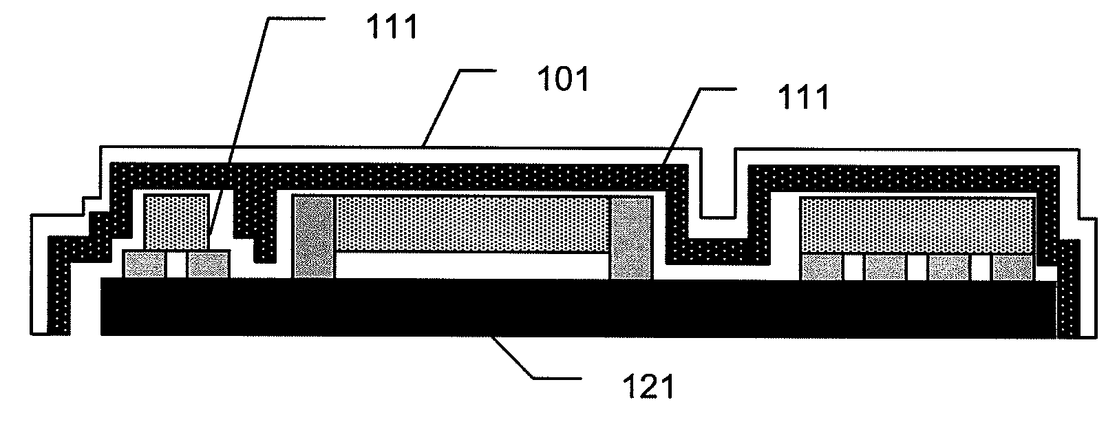
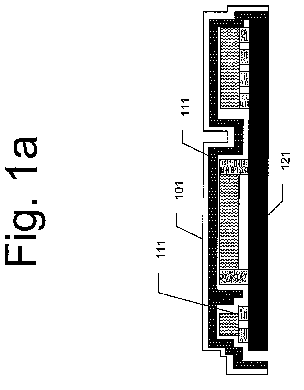
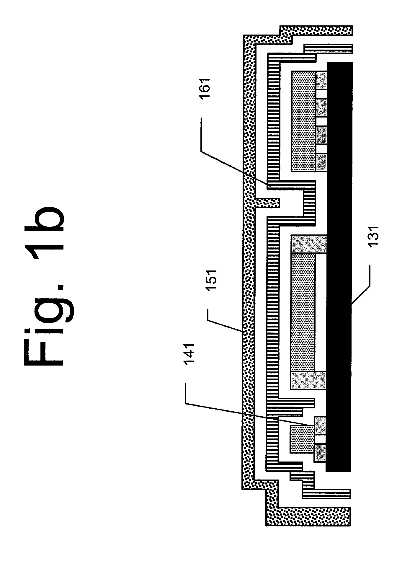
[0039]In one variation, a conformal electro-magnetic shield for an electronic or electro-optical component or component group may include at least an electrically insulating layer disposed onto the component surface and an electrically conductive shielding layer disposed on top of the insulating layer.

[0040]Some such variations may include an elastomeric insulating layer such as silicone, elastomer, resin, latex, rubber, and similar flexible substances. Such variations of an insulating layer may be configured, based on the material properties of the layer and the underlying component(s), to be easily removable such that the underlying compon...


PUM

PropertyMeasurementUnit
electrically conductiveaaaaaaaaaa
electricallyaaaaaaaaaa
thresholdaaaaaaaaaa

Abstract

A conformal electro-magnetic (EM) shield and a method of applying such a shield are provided herein as well as variations thereof. Variations include, but are not limited to, frequency-selective shielding, shields containing active and / or passive electronic components, and strippable shields that can easily be applied to and removed from underlying components. Variations of a shield structure include at least an insulating layer between the underling component and the shield, and shielding and / or capping layers disposed over the insulating layer.

Description

[0001]The present invention claims benefit of priority to Provisional Application 61 / 251,565, filed in the U.S. Patent and Trademark Office on Oct. 14, 2009, the entire contents of which are hereby incorporated by reference. The present invention also claims benefit of priority to Provisional Application 61 / 348,156, filed in the U.S. Patent and Trademark Office on May 25, 2010, the entire contents of which are hereby incorporated by reference.FIELD OF THE INVENTION[0002]The present invention relates generally to electromagnetic and radio-frequency shielding solutions to protect components or information stored in electronic or optical modules, components of a printed circuit or wiring board, or in integrated circuits or optical devices.BACKGROUND OF THE INVENTION[0003]Electromagnetic (EM) interference can cause detrimental effects on electronic systems. These effects may range from unwanted noise to critical system failures or information loss. In order to avoid these problems, it i...

Claims


Application Information

Patent Timeline
Patent Type & Authority Applications(United States)
IPC IPC(8): H05K9/00H01B19/00
CPCH05K1/0275H01L2924/09701Y10T29/49227H05K3/284H01L2924/3011H01L23/573H01L23/57H01L2924/0002H01L2924/00H01L23/576G06F21/73
Inventor KELLEY, MATTHEWADAMS, CHRISTIANNELSON, PATRICK A.
Owner LOCKHEED MARTIN CORP
Why Eureka
Try Eureka