Laminated electronic component

a technology of electronic components and laminates, applied in the direction of fixed capacitor details, capacitors, capacitors, etc., can solve the problemslimiting the amount of ceramic layer that can be increased within a specified dimensional standard of the product, and affecting the quality of the product. , to achieve the effect of reducing the thickness of the ceramic layer, reducing the risk of short circuit between internal electrodes, and ensuring the quality of the produ

Active Publication Date: 2011-05-26
MURATA MFG CO LTD
View PDF18 Cites 22 Cited by
  • Summary
  • Abstract
  • Description
  • Claims
  • Application Information

AI Technical Summary

Benefits of technology

[0010]To overcome the problems described above, preferred embodiments of the present invention provide a laminated electronic component including an external terminal electrode formed by direct plating on an outer surface of an electronic component body that is less likely to have deteriorated characteristics and that has excellent durability.
[0013]According to a preferred embodiment of the present invention, since the grain diameters of the metal grains defining the plating film are very small, a specific surface area of the surface of the plating film is increased, and even if there is a gap between the electronic component base material and the plating film, the gap is more likely to be filled by oxidation expansion of the plating film in the vicinity of the gap. Therefore, the entry of water is effectively prevented, and a laminated electronic component having excellent reliability is obtained.
[0014]Further, according to a preferred embodiment of the present invention, since the grain diameters of the metal grains defining the plating film are very small, activity with respect to the plating precipitating thereon is increased, and an upper layer plating film having a uniform thickness is obtained. In other words, the in-plane variations in film thickness of the upper layer plating are very small, such that the continuity of the plating film is less likely to decrease even if the thickness of the upper layer plating film is reduced.
[0015]Further, the metal grains defining the plating film are preferably Cu grains, for example. This is because Cu plating has a high throwing power with respect to an object to be plated, and even if the electronic component body has a large surface roughness, a gap is less likely to occur between the electronic component body and the plating film.

Problems solved by technology

However, when the thickness of the ceramic layer is further reduced, a short circuit between internal electrodes is likely to occur.
However, there is a limit to the amount that the ceramic layer can be increased within a specified dimensional standard of the product, and the thickness of the external terminal electrode will prevent further increases in the area of the ceramic layer.
However, with this method, the conductive paste is likely to be thicker in a central portion of the ceramic base material end surface due to the influence of viscosity of the conductive paste.
Therefore, the thickness of the external terminal electrode partially increases, e.g., to greater than 30 μm, and it is not possible to sufficiently reduce the volume of the ceramic base material.
However, when forming an external terminal electrode on the outer surface of an electronic component body, i.e., a ceramic base material, by direct plating, when an average grain diameter of metal grains in a plating film used to form the external terminal electrode is increased, a problem arises in that water enters through a gap between the electronic component body and the plating film.
Further, when the thickness of the plating film is reduced, there is a problem in that the continuity of the plating film is deteriorated due to a reduced smoothness of the plating film.
In these cases, there is a problem in that reliability is decreased, for example, the insulation resistance is decreased over time.

Method used


Image

  • Laminated electronic component
  • Laminated electronic component
  • Laminated electronic component

Examples


first preferred embodiment

[0027]In a first preferred embodiment of the present invention, a two-terminal laminated ceramic capacitor including a pair of external terminal electrodes defined by plating film layers is described as an example of a laminated electronic component.

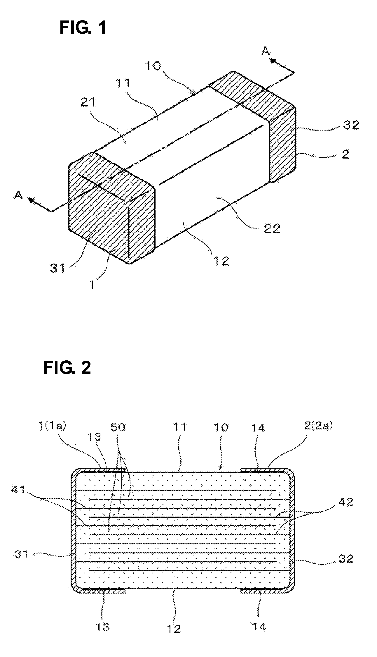
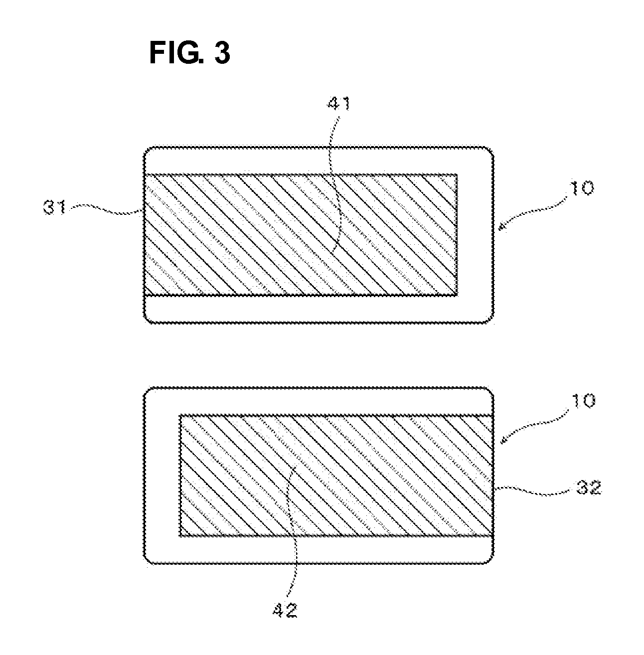
[0028]FIG. 1 is a perspective view showing a laminated ceramic capacitor according to the first preferred embodiment of the present invention, FIG. 2 is a cross section view along the line A-A in FIG. 1, FIG. 3 is a view showing an internal electrode pattern of the laminated ceramic capacitor, and FIG. 4 is an enlarged view of a connecting portion between an external terminal electrode and an internal electrode.

[0029]The laminated ceramic capacitor includes a capacitor body 10 preferably having a substantially rectangular parallelepiped shape including a first main surface 11 and a second main surface 12 that are opposed to each other, a first lateral surface 21 and a second lateral surface 22 that are opposed to each other, and a first ...

second preferred embodiment

[0066]FIG. 5 is an enlarged view of a portion of a laminated ceramic capacitor according to a second preferred embodiment of the present invention. The laminated ceramic capacitor of the second preferred embodiment is similar to the laminated ceramic capacitor of the first preferred embodiment, except that the first (and the second) external terminal electrodes 1 (2) are defined only of the plating films 1a (2a).

[0067]In FIG. 5 shows the connecting portion between the first external terminal electrode 1 provided on the first end surface 31 of the capacitor body 10 and the first internal electrode 41. However, the connecting portion between the second external terminal electrode 2 (see FIGS. 1 and 2) and the second internal electrode 42 is substantially the same as that shown in FIG. 5, and thus, the plating film 2a, the second internal electrode 42 and other elements defining the second external terminal electrode 2 are also shown in parentheses.

[0068]The laminated ceramic capacitor...

third preferred embodiment

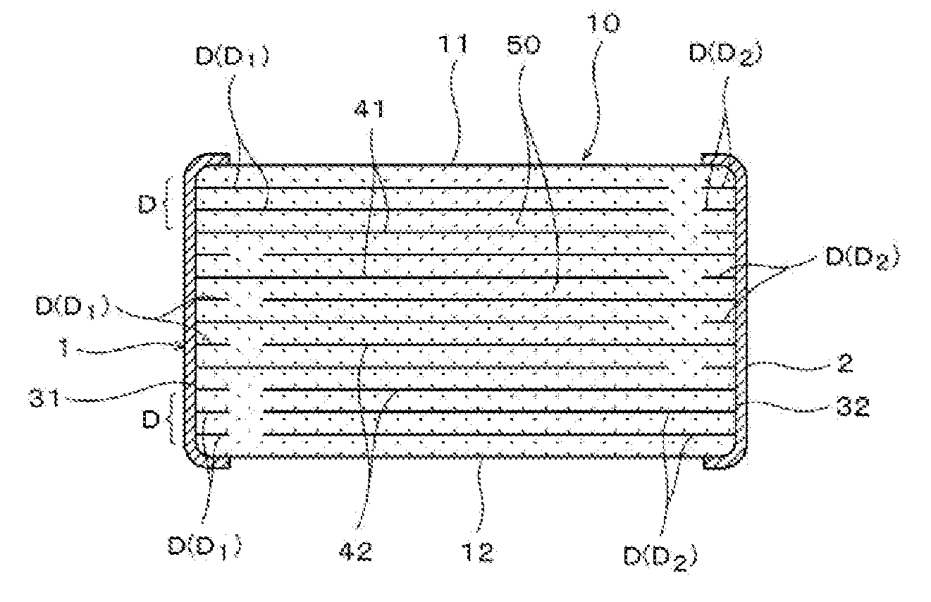
[0070]FIG. 6 shows a laminated ceramic capacitor according to a third preferred embodiment of the present invention. The laminated ceramic capacitor of the third preferred embodiment is configured similarly to the laminated ceramic capacitor of the first preferred embodiment, except that the capacitor body 10 includes dummy internal electrodes D (D1 and D2). In FIG. 6, the portions denoted by the same reference numerals as in FIG. 2 represents the same or similar portions.

[0071]In this laminated ceramic capacitor, a first dummy internal electrode D1 extending to the first end surface 31 and a second dummy internal electrode D2 extending to the second end surface 32 preferably are provided. The first and second dummy internal electrodes D1 and D2 are arranged on the same or substantially the same plane as the internal electrodes 41 and 42 disposed between the dielectric layers 50, and are also arranged in the outer layer portion at which the internal electrode is not provided on the ...


PUM


Abstract

A laminated electronic component includes a component body including a plurality of laminated functional layers, a plurality of internal conductors provided inside the component body, and an external terminal electrode that is electrically connected to an internal conductor via an exposed portion of the internal conductor and that is defined by a direct plating film. An average grain diameter of metal grains defining the plating film is about 0.1 μm or less.

Description

BACKGROUND OF THE INVENTION[0001]1. Field of the Invention[0002]The present invention relates to a laminated electronic component and a method of producing the same, and more particularly, to a laminated electronic component in which an external terminal electrode connected with an internal conductor is formed through a step of direct plating on an outer surface of an electronic component body.[0003]2. Description of the Related Art[0004]Recently, the market for small-sized portable electronic instruments, such as mobile phones, notebook personal computers, digital cameras, and digital audio instruments has been expanding. In such portable electronic instruments, not only is the size getting smaller, but also the performance is getting higher. Such a portable electronic instrument is equipped with a plurality of laminated ceramic electronic components, and smaller size and higher performance are also desired for these laminated ceramic electronic components. In a laminated ceramic c...

Claims


Application Information

Patent Timeline
Patent Type & Authority Applications(United States)
IPC IPC(8): H01G4/008
CPCH01G4/30H01G4/2325
Inventor OGAWA, MAKOTOMOTOKI, AKIHIROTAKEUCHI, SYUNSUKEKAWASAKI, KENICHI
Owner MURATA MFG CO LTD
Why Eureka
Try Eureka