
Eureka
For R&D, Eureka makes reading and utilizing patents & technical documents easy.
Eureka AIR
Designed for self-driven R&D workflows. Generate viable solutions, solve complex R&D challenges, empower your innovation with AI.

Eureka Materials
Designed for material experts only. Revolutionize your material R&D, from search, analyze, to developing new materials.

TechResearch
Generate reliable direction feasibility study reports for your R&D in just a few steps.

TechSeek
Discover and master advanced knowledge NOW. Basics, ideas, possibilities, all at once.

TechMind
As an expert in R&D Theories, TechMind can generates customized viable solutions instantly.

TechRisk
Analyze your overall solution with one click, know your potential R&D risks in advance.

TechMonitor
Get weekly tech updates, stay abreast of the latest tech innovations and key insights.
Self aligned carbide source/drain fet
- Summary
- Abstract
- Description
- Claims
- Application Information
AI Technical Summary
Benefits of technology
Problems solved by technology
Method used
Image

Examples
Embodiment Construction
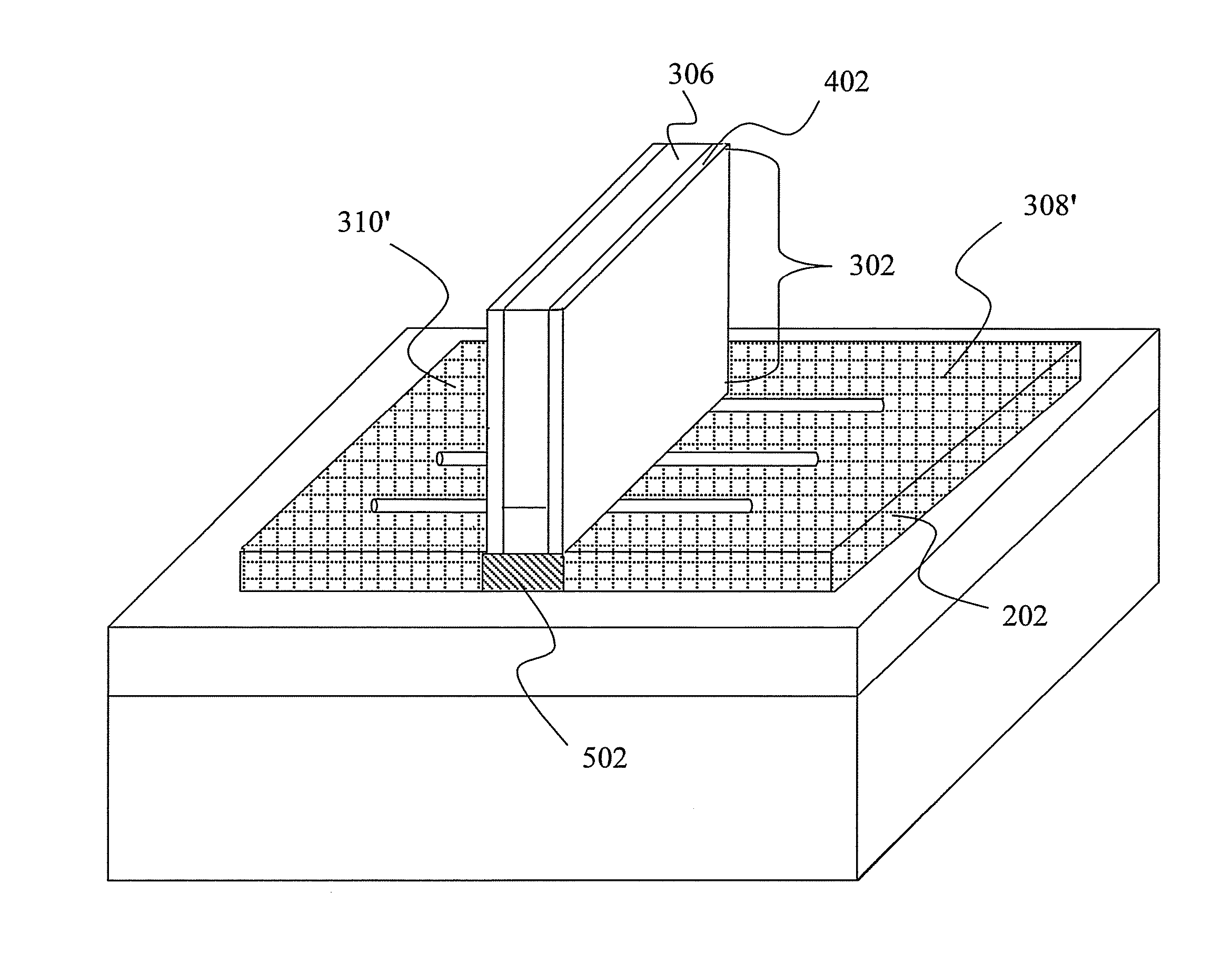
One embodiment of the present invention is directed to a self-aligned carbide source / drain contact formation process for a FET having a nanostructure based channel region. In particular, disclosed herein is a platform for building self-aligned devices from any deposited nanostructure, including carbon nanotubes, graphene, or semiconducting nanowires. The nanostructures are deposited on an insulating carbon underlayer, and a gate stack is patterned atop the nanostructures. Metal is then deposited everywhere. Any region of the carbon under-layer not protected by the gate stack is converted to a metal carbide contact, and the metal is then removed selectively to the metal carbide contacts, resulting in metal carbide source / drain contacts which are self-aligned to the gate stack.
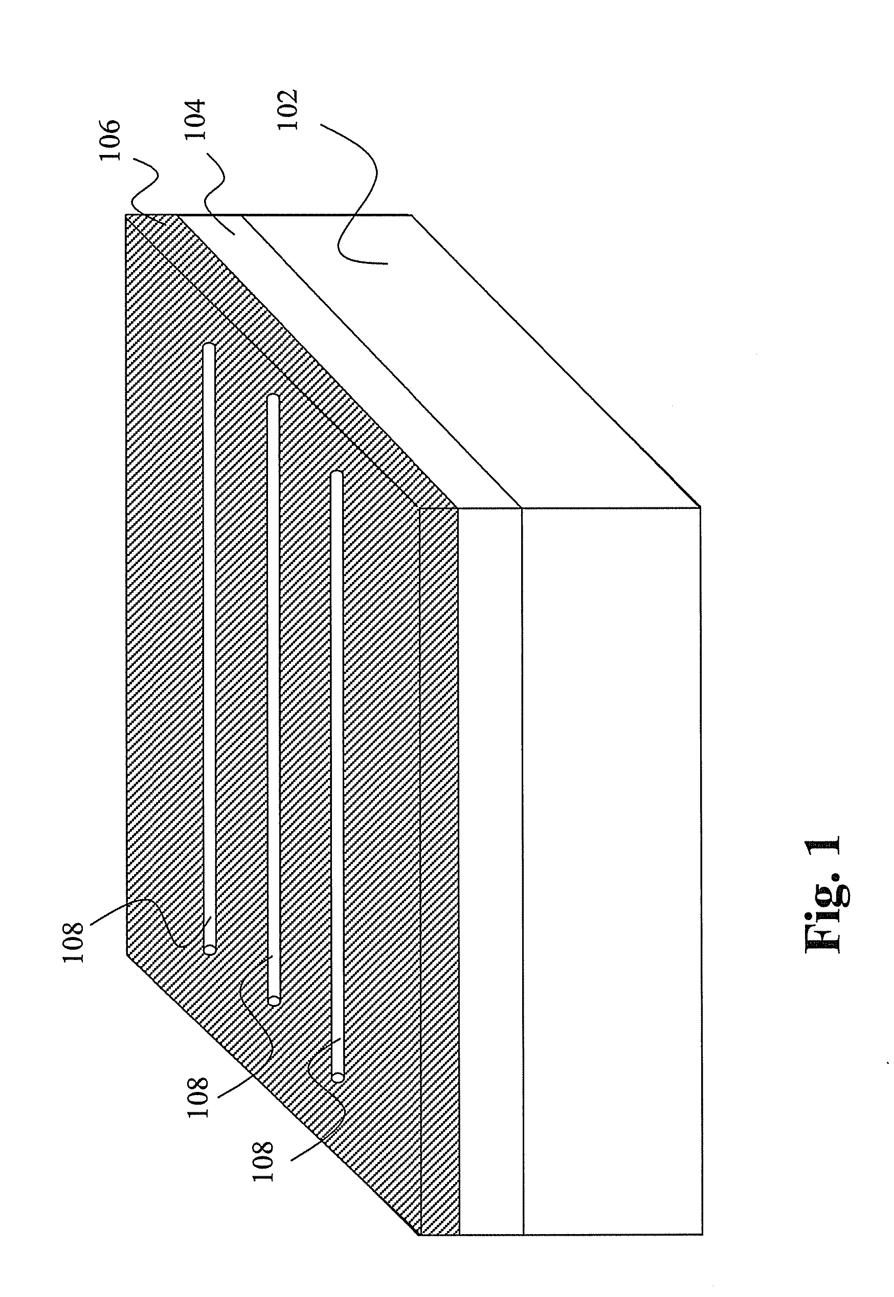
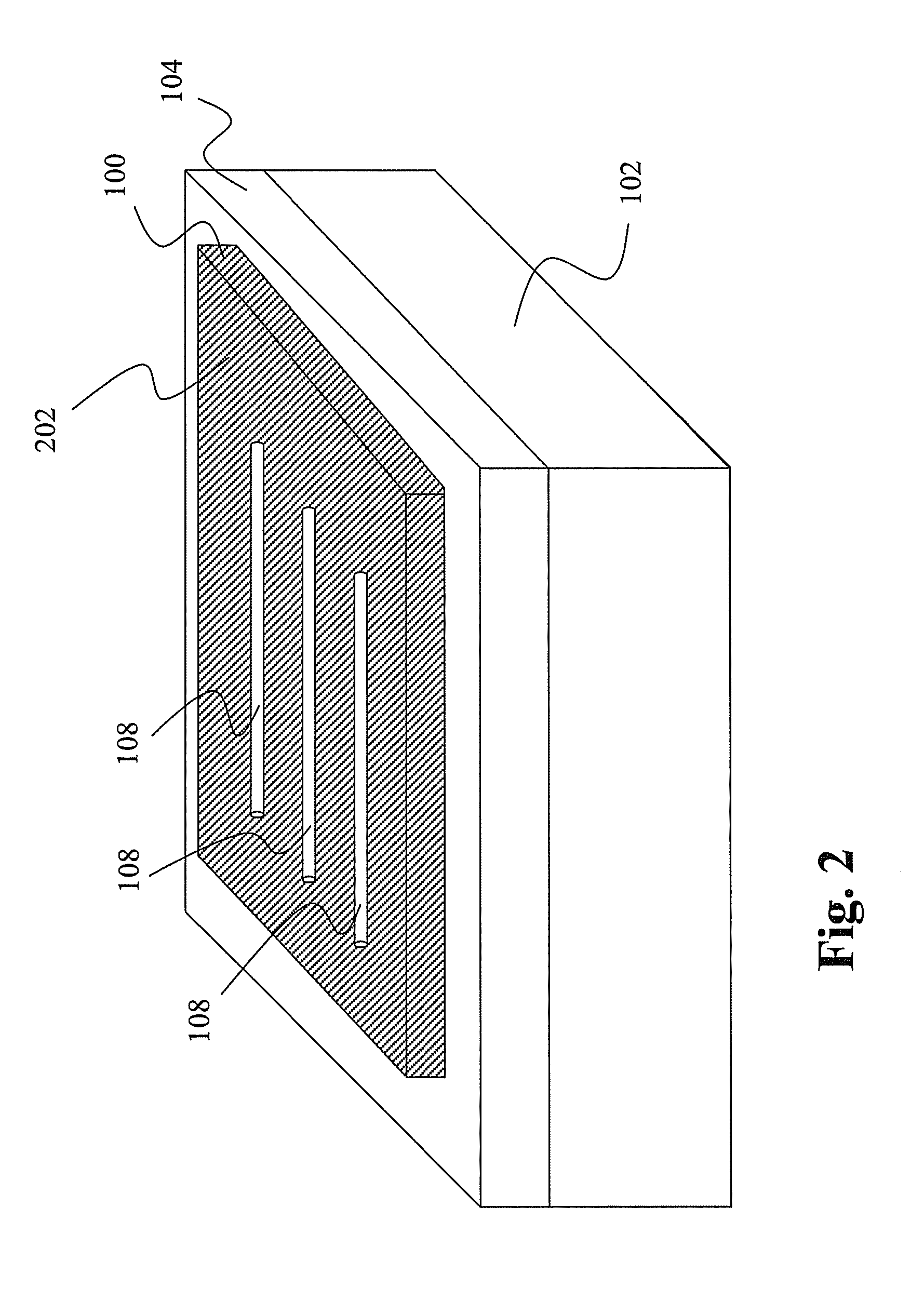
With reference now to FIG. 1, an example of a wafer in the production process of a FET according to one embodiment of the present invention is shown. The wafer includes a substrate 102. The substrate 102 may be ...
PUM
 Abstract
Description
Claims
Application Information
 - R&D Engineer
- R&D Manager
- IP Professional
- Industry Leading Data Capabilities
- Powerful AI technology
- Patent DNA Extraction
Browse by: Latest US Patents, China's latest patents, Technical Efficacy Thesaurus, Application Domain, Technology Topic, Popular Technical Reports.
© 2024 PatSnap. All rights reserved.Legal|Privacy policy|Modern Slavery Act Transparency Statement|Sitemap|About US| Contact US: help@patsnap.com