Non-Inductive Resistor and the Manufacturing Method Thereof

a manufacturing method and resistor technology, applied in the direction of resistor manufacturing, adjustable resistors, resistors, etc., can solve the problems of noise generation, undesirable noise, and noise produced by inductance effects

Inactive Publication Date: 2011-06-02
FUTABA ELECTRIC
View PDF7 Cites 4 Cited by
  • Summary
  • Abstract
  • Description
  • Claims
  • Application Information

AI Technical Summary

Benefits of technology

[0012]The main object of the present invention is to provide a type of non-inductive resistor, wherein an inductance effect of the non-inductive resistor is counteracted by a clockwise cut mark and a counterclockwise cut mark.

Problems solved by technology

According to Flemming's right hand rule, an inductance effect is created at the center of the current rotation, and this inductance effect produces noise when the circuit is powered on or produces undesirable noise in the speaker of the audio system.
As a result, noise will be produced.
However, the prior invention has its technical limitations.
For example, the non-inductive wire-wound cannot be used where precision or high resistance is required.
Because the non-inductive cutting method cannot cut the resistor for more than half cycle of rod, the material utilization rate of this method is only 20%˜30%; this low rate will result in too much waste material.
The manufacturing limitation of the print pattern method is that it is inapplicable to the make of small sized products; another weakness is that each of the products needs to be modified and etched after the printing process of conductive layer to produce the required resistance and standard deviation.
This is a problem when mass production and cost considerations.
However, if the materials' initial resistance substantially deviates from the resistance of the final product, the time needed for etching is drastically increased; as a result, this technology tends to cause difficulties during mass production.

Method used


Image

  • Non-Inductive Resistor and the Manufacturing Method Thereof
  • Non-Inductive Resistor and the Manufacturing Method Thereof
  • Non-Inductive Resistor and the Manufacturing Method Thereof

Examples


Embodiment Construction

[0020]The advantages and innovative features of the invention will become more apparent from the following preferred embodiments.

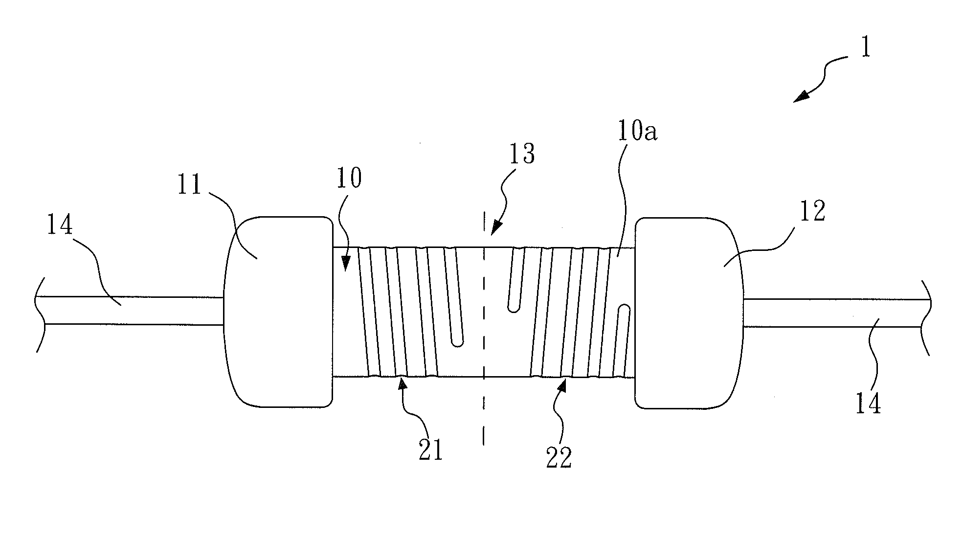
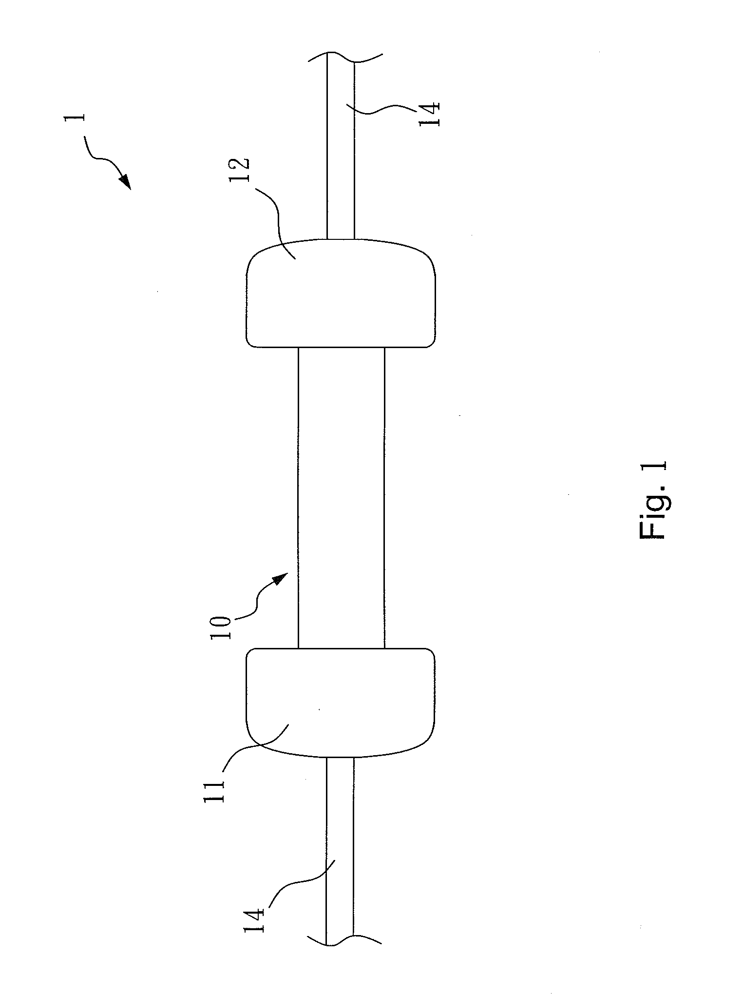
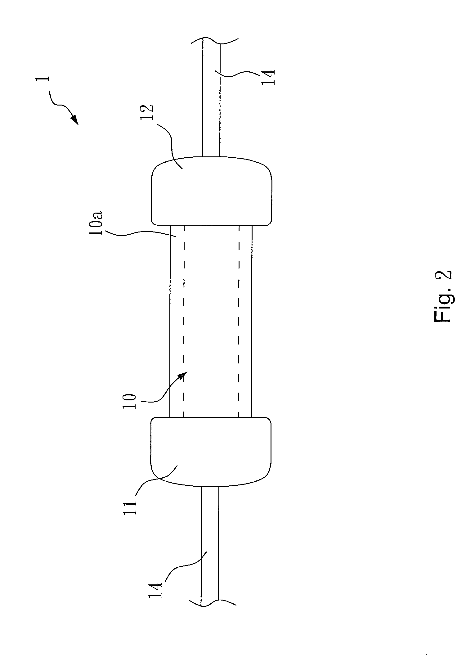
[0021]Please refer to FIG. 1, FIG. 2 and FIG. 3 of the non-inductive resistor of the present invention. FIG. 1 is a diagram of the rod. FIG. 2 is a diagram of the conductive layer covering the rod. FIG. 3 is a diagram of the non-inductive resistor.

[0022]The non-inductive resistor 1 of the present invention is a film type resistor. The non-inductive resistor 1 comprises: a resistance rod 10, a conductive layer 10a, a clockwise cut mark 21, and a counterclockwise cut mark 22. As shown in FIG. 1, the resistance rod 10 comprises a first end 11 and a second end 12. The first end 11 and the second end 12 are mounted on the end cap by gluing or welding, and are respectively connected to a metallic conducting wire 14, thus enabling the non-inductive resistor 1 to be electrically connected to an outer electrical component (not shown).

[0023]As shown in FIG. 2, the r...


PUM

PropertyMeasurementUnit
resistanceaaaaaaaaaa
conductiveaaaaaaaaaa
inductanceaaaaaaaaaa

Abstract

A non-inductive resistor and a method of manufacturing a non-inductive resistor are disclosed. The non-inductive resistor comprises a resistance rod, a conductive layer, a clockwise cut mark, and a counterclockwise cut mark. The resistance rod comprises a first end and a second end, and a cutting center is established between the first end and the second end. The conductive layer is used for covering the resistance rod between the first end and the second end. The clockwise cut mark is situated on the conductive layer between the first end and the cutting center. The counterclockwise cut mark is situated on the conductive layer between the second end and the cutting center, wherein the clockwise cut mark and counterclockwise cut mark are used for counteracting an inductance effect of the non-inductive resistor.

Description

BACKGROUND OF THE INVENTION[0001]1. Field of the Invention[0002]The present invention relates to a non-inductive resistor and its manufacturing method, and more particularly, to a type of non-inductive resistor which has clockwise and counterclockwise cut marks, and the manufacturing method of the non-inductive resistor.[0003]2. Description of Related Art[0004]The resistor is one of the basic components in electronic devices or on circuit boards. The main function of the resistor is to regulate current or voltage in the circuit. During the process of cutting or etching of the traditional resistor, and whether the process utilizes the diamond blade cutting or laser etching, a number of circular loops will be created on the electronic circuit; a current rotation effect will be created when the current passes through the conductive layer of the resistor. According to Flemming's right hand rule, an inductance effect is created at the center of the current rotation, and this inductance e...

Claims


Application Information

Patent Timeline
Patent Type & Authority Applications(United States)
IPC IPC(8): H01C3/02H01C17/00
CPCH01C3/02Y10T29/49082H01C17/24H01C7/001
Inventor LIAO, CHIN-CHUNG
Owner FUTABA ELECTRIC
Why Eureka
Try Eureka