

Stacked inductor with multi paths for current compensation
a multi-path, current compensation technology, applied in the field of microelectronics, can solve the problems of increasing current paths, reducing resistance, and non-uniformity of inner and outer current density, so as to reduce the impact of skin effect and current crowding effect, increase inductance, and maintain high q factor.
- Summary
- Abstract
- Description
- Claims
- Application Information
AI Technical Summary
Benefits of technology
Problems solved by technology
Method used
Image

Examples
Embodiment Construction
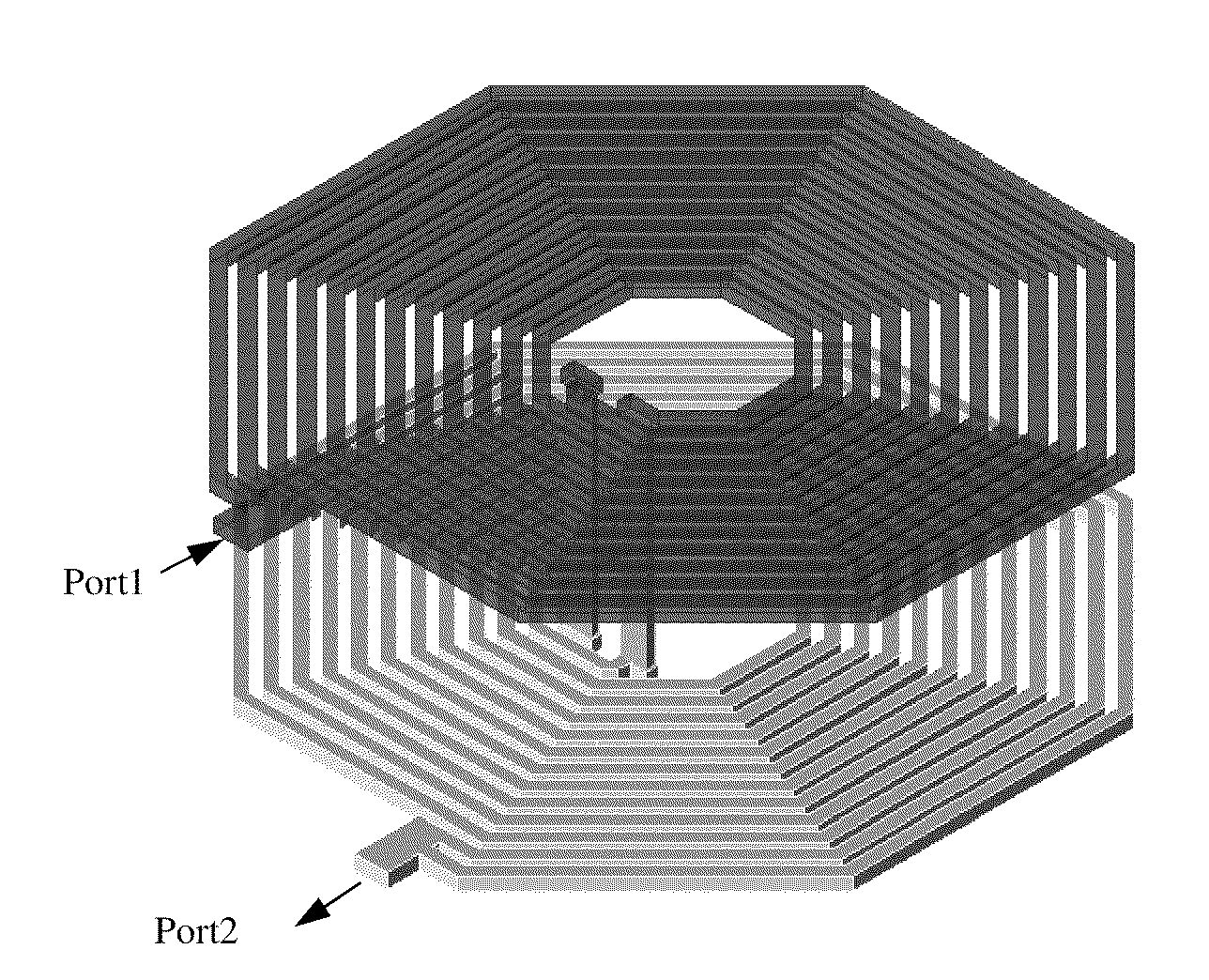
[0027]This multi paths stacked inductor for current compensation comprises top and bottom metal trace, which are aligned with each other, each metal trace consists of multi paths. The inner path the inner path of the top metal trace flips over to the outer path when connected to the bottom metal trace, the outer path of the bottom metal trace flips over to the inner path when connected to the top metal trace; These paths join together at the end of the metal trace with via holes.
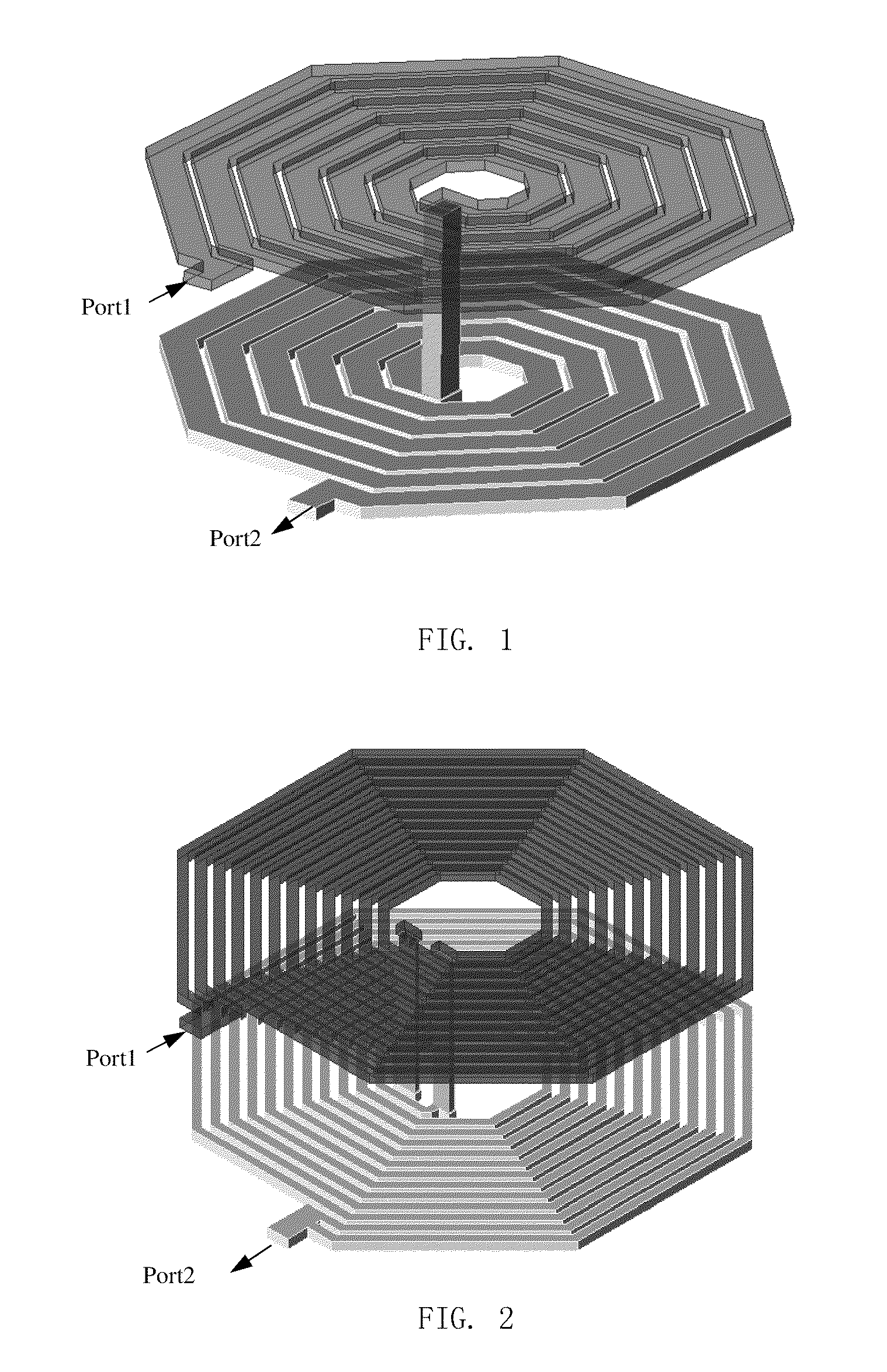
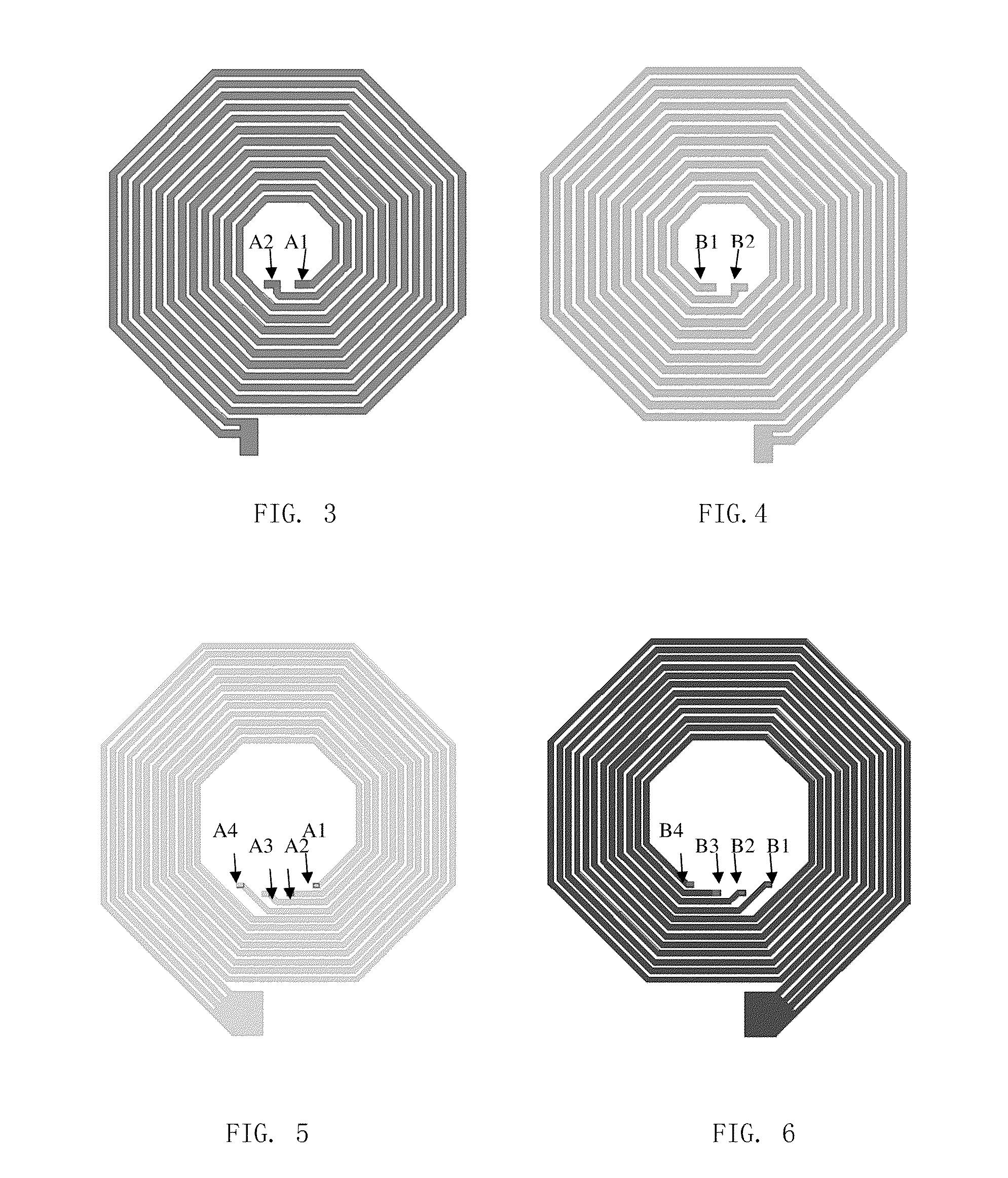
[0028]More detailed the layout of stacked inductor with top and bottom metal trace aligned with each other (taking two layer, 6 turns, and octagonal stacked inductor for example) is shown in FIG. 3 and FIG. 4, with stereogram in FIG. 2. The width and thickness of the two layer metal trace is equal in FIG. 2. Also from FIG. 2, each metal trace has multi paths, with the inner path in top metal flips over to the outer path in the bottom metal, while the outer path in top metal flips over to the inner path in th...
PUM
 Abstract
Description
Claims
Application Information