Method and Apparatus for Manufacturing Thin-Film Transistor

a thin film transistor and manufacturing method technology, applied in the direction of manufacturing tools, solid-state devices, laser beam welding apparatus, etc., can solve the problems of reducing the yield of tft, deteriorating productivity, and damage to the semiconductor layer, so as to reduce the time of fabrication, prevent the damage of the semiconductor layer, and simplify the process of fabricating the tft array substrate

Active Publication Date: 2011-06-09
MOOHAN
View PDF6 Cites 12 Cited by
  • Summary
  • Abstract
  • Description
  • Claims
  • Application Information

AI Technical Summary

Benefits of technology

[0014]An aspect of the present invention is to provide a method and apparatus of fabricating TFT, which patterns an ohmic contact layer by a laser patterning process so that it is capable of preventing a semiconductor layer from being damaged, and reducing fabrication time.
[0015]Another aspect of the present invention is to provide a method and apparatus of fabricating TFT, which is capable of simplifying a process of fabricating a TFT array substrate, and preventing a semiconductor layer from being damaged.
[0016]Another aspect of the present invention is to provide a method and apparatus of fabricating TFT, which is capable of simplifying a process of patterning a thin film, and reducing patterning time.

Problems solved by technology

Since the ohmic contact layer is selectively etched by the dry etching process, an inaccurate etching for the ohmic contact layer may cause a problem of over etching, whereby the semiconductor layer may be damaged due to the over etching.
Also, the damage to the semiconductor layer may lower the yield of TFT.
As the ohmic contact layer is selectively etched by the dry etching process, the increased fabrication time causes deterioration of productivity.
Since the pixel electrode is electrically connected with the source electrode by photolithography, the fabrication process is complicated and the fabrication time is increased, thereby lowering the yield.

Method used


Image

  • Method and Apparatus for Manufacturing Thin-Film Transistor
  • Method and Apparatus for Manufacturing Thin-Film Transistor
  • Method and Apparatus for Manufacturing Thin-Film Transistor

Examples


first embodiment

[0073]FIG. 2 is a perspective view illustrating an apparatus of fabricating TFT according to the present invention.

[0074]Referring to FIG. 2, the apparatus of fabricating TFT according the first embodiment of the present invention includes a base frame 1100, a stage 1110, a gantry 1200, and a laser irradiation apparatus 200.

[0075]The base frame 1100 supports the stage 1110. Inside the base frame 1100, there may be a driving / controlling apparatus (not shown) which drives and controls the stage 1110, the gantry 1200, and the laser irradiation apparatus 200, respectively.

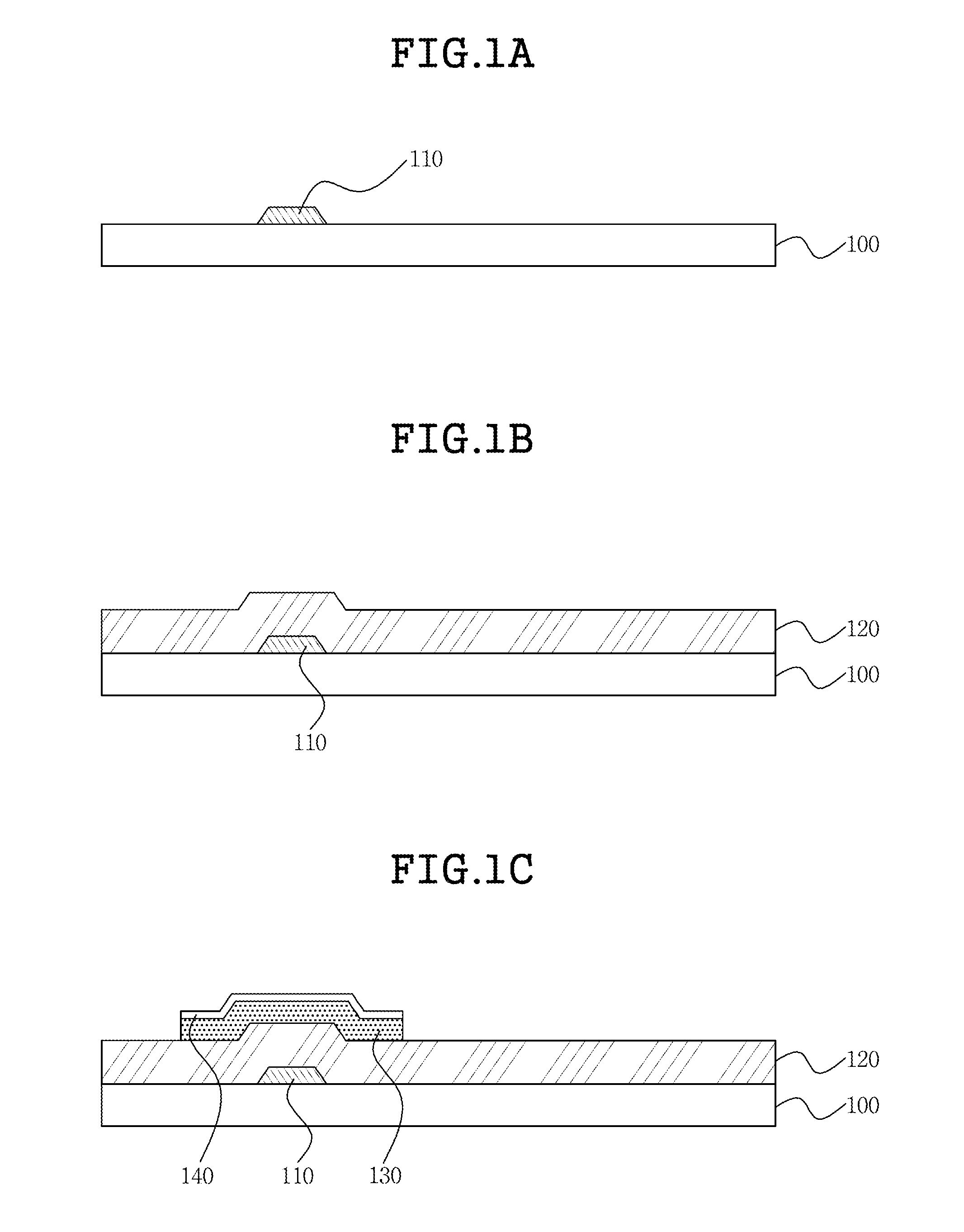
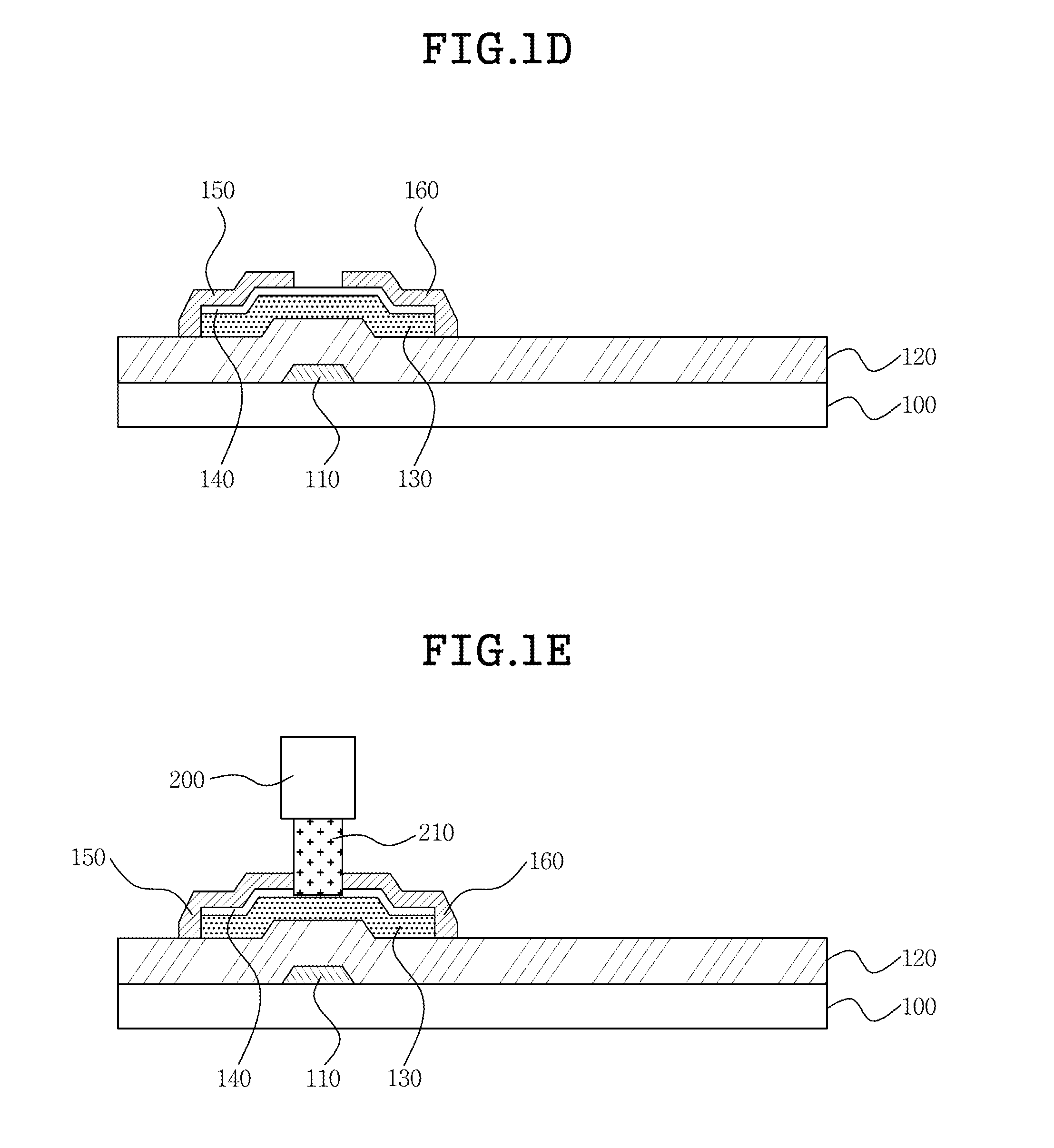
[0076]The substrate 100 is transferred by an external substrate-transfer (not shown), and the transferred substrate 100 is loaded on the stage 1110. At this time, the external substrate-transfer (not shown) loads the substrate 100 which completes cleaning and drying processes after forming the source and drain electrode patterns 160 and 150 by the aforementioned steps of FIG. 1(A to D), onto the stage 1110.

[0077]The st...

second embodiment

[0085]FIG. 3 is a perspective view illustrating an apparatus of fabricating TFT according to the present invention.

[0086]Referring to FIG. 3, the apparatus of fabricating TFT according to the second embodiment of the present invention includes a base frame 1100, a stage 1110, a gantry 1200, and a plurality of laser irradiation apparatuses 200. Except that the apparatus of fabricating TFT according to the second embodiment of the present invention is provided with the plurality of laser irradiation apparatuses 200 in the gantry 1200 so as to reduce fabrication time, the apparatus of fabricating TFT according to the second embodiment of the present invention is identical in structure to the apparatus of fabricating TFT according to the first embodiment of the present invention. Thus, an explanation will be provided only concerning different structures from those of the first embodiment of the present invention, that is, the aforementioned explanation for the same structures can substi...

third embodiment

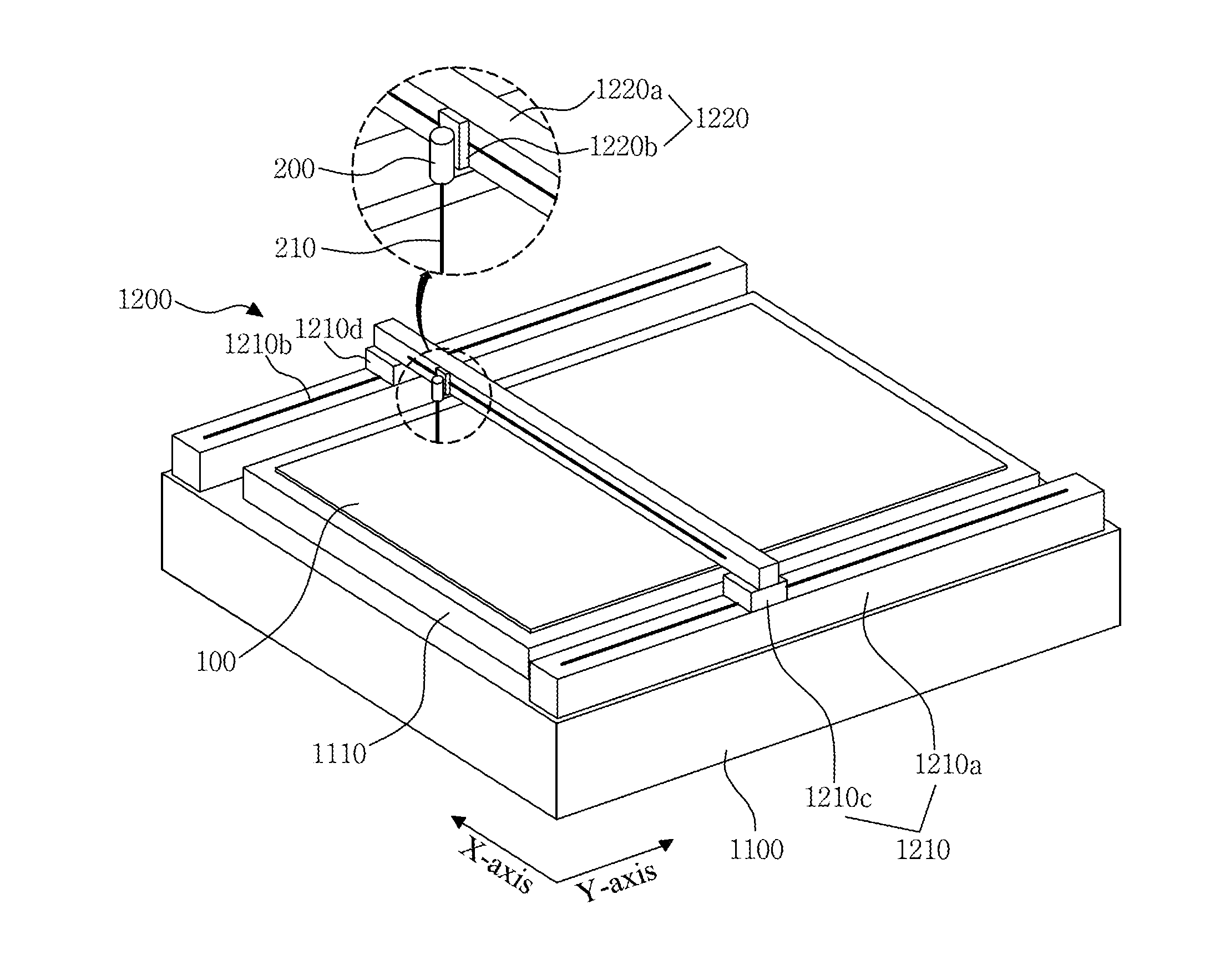
[0091]FIG. 4 illustrates an apparatus of fabricating TFT according to the present invention.

[0092]Referring to FIG. 4, the apparatus of fabricating TFT according to the third embodiment of the present invention is provided with a plurality of laser irradiation apparatuses 200 arranged along the Y-axis direction and the X-axis direction to reduce fabrication time. Thus, an explanation will be provided only concerning different structures from those of the first embodiment of the present invention, that is, the aforementioned explanation for the same structures can substitute for the detailed explanation for the structures of the apparatus according to the third embodiment of the present invention.

[0093]A gantry 1200 may comprise a first gantry 1210 installed on a base frame 1100; and a plurality of second gantries 1220, installed in the first gantry 1210 and provided at fixed intervals, for moving the plurality of laser irradiation apparatuses 200 in the X-axis direction.

[0094]The fi...


PUM

PropertyMeasurementUnit
infrared wavelengthaaaaaaaaaa
semiconductoraaaaaaaaaa
widthaaaaaaaaaa

Abstract

A method and apparatus of fabricating a thin film transistor is disclosed, which patterns an ohmic contact layer by a laser patterning process so that it is capable of preventing a semiconductor layer from being damaged, and reducing fabrication time, wherein the method comprises forming a gate electrode pattern on a substrate; forming a gate insulating layer on the gate electrode pattern; sequentially forming a semiconductor layer pattern and an ohmic contact layer pattern on the gate insulating layer; forming source and drain electrode patterns on the ohmic contact layer pattern, wherein the source and drain electrode patterns are provided at a fixed interval therebetween; and removing the ohmic contact layer pattern exposed between the source and drain electrode patterns through the use of laser.

Description

CROSS REFERENCE TO RELATED APPLICATIONS[0001]This application claims the benefit of the Korean Patent Application Nos. P2008-0075640, P2008-0075652, and P2008-0075669 filed on Aug. 1, 2008, which are hereby incorporated by reference as if fully set forth herein.BACKGROUND OF THE INVENTION[0002]1. Field of the Invention[0003]The present invention relates to a method and apparatus of fabricating a thin film transistor, and more particularly, to a method and apparatus of fabricating a thin film transistor, which patterns an ohmic contact layer by a laser patterning process so that it is capable of preventing a semiconductor layer from being damaged, and reducing fabrication time.[0004]2. Discussion of the Related Art[0005]Generally, a thin film transistor (hereinafter, referred to as “TFT”) may be used as a switching device for controlling an operation of each pixel in a flat type display device such as a liquid crystal display device or a light-emitting display device; or may be used ...

Claims


Application Information

Patent Timeline
Patent Type & Authority Applications(United States)
IPC IPC(8): H01L21/336B23K26/00
CPCH01L29/66765H01L27/1288H01L27/124
Inventor LEE, HYUNG SUP
Owner MOOHAN
Why Eureka
Try Eureka