Semiconductor device and production method thereof

a technology of a semiconductor device and a production method, applied in the direction of semiconductor devices, basic electric elements, electrical appliances, etc., can solve the problems of weakening of the strain in the channel region and difficulty in applying a strong strain to the channel region, and achieve the effect of improving device characteristics and strong strain

Active Publication Date: 2011-06-23
RENESAS ELECTRONICS CORP
View PDF12 Cites 21 Cited by
  • Summary
  • Abstract
  • Description
  • Claims
  • Application Information

AI Technical Summary

Benefits of technology

[0017]Furthermore, in a semiconductor device according to the present invention, the upper part of a gate electrode is not covered with a stress applying film. Consequently, it can be avoided that a strain is generated in a direction opposite to an intended direction in a channel region and that makes it difficult to apply a strong strain to the channel region.
[0018]That is, a semiconductor device according to the present invention makes it possible to apply a strong uniaxial strain to a channel region of the semiconductor device and improve device characteristics.
[0019]The present invention makes it possible to apply a strong strain to a channel region.

Problems solved by technology

Conventional methods have following problems.
It has been difficult to apply a strong strain to a channel region because the upper part of a gate electrode is covered with a stress applying film and strain is generated therefore in a direction opposite to an intended direction in the channel region.
Meanwhile, a problem has been that a stress applying film is exfoliated from the surface of an FET and that causes strain in a channel region to weaken when a true stress caused by the stress applying film is large or when stress applied to the interface between the stress applying film and the surface of the FET is enhanced by using a structure of removing the stress applying film over the upper part of a gate electrode as described in S. Yamakawa et al., “Study of Stress Effect on Replacement Gate Technology with Compressive Stress Liner and eSiGe for pFETs”, Proceedings of 2008 International Conference on Simulation of Semiconductor Processes and Devices, The Institute of Electrical and Electronics Engineers, Inc., 109-112 (2008).

Method used


Image

  • Semiconductor device and production method thereof
  • Semiconductor device and production method thereof
  • Semiconductor device and production method thereof

Examples


first exemplary embodiment

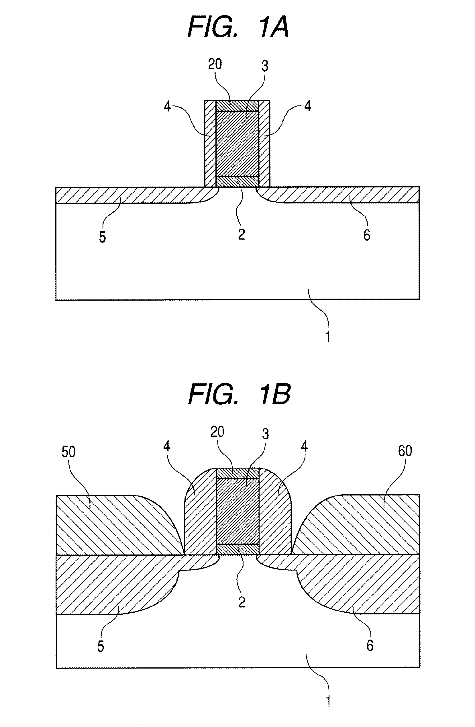
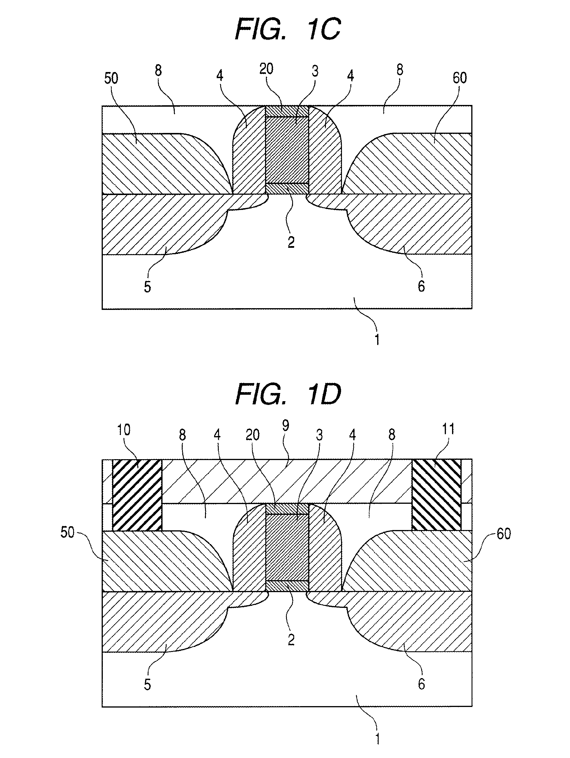
[0045]A sectional view of an example of a semiconductor device according to a first exemplary embodiment of the present invention is shown in FIG. 1D.

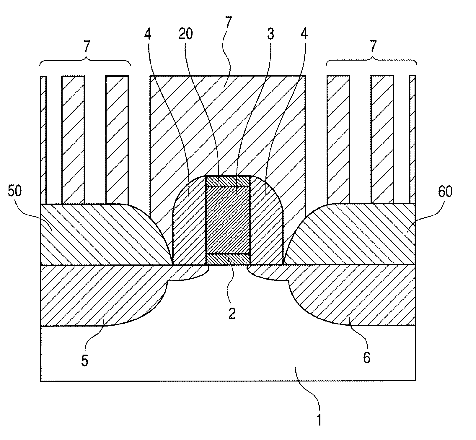
[0046]As shown in the figure, a semiconductor device according to the present embodiment includes: a semiconductor substrate 1; a gate insulating film 2 formed over a first plane (a plane on the upside in the figure) of the semiconductor substrate 1; a gate electrode 3 formed over the gate insulating film 2; a gate sidewall insulating film 4 formed over the sidewall of the gate electrode 3; a source / drain diffusion layer region 5, 6, being adjacent to a channel region formed in the semiconductor substrate 1 below the gate electrode 3, into which impurities are implanted; protrusions 50 and 60 or recesses (not shown in the figure) formed in a region where the source / drain diffusion layer region 5, 6 is formed over the first plane (the plane on the upside in the figure) of the semiconductor substrate 1; and a stress applying film 8 forme...

second exemplary embodiment

[0074]The present embodiment is based on the first exemplary embodiment but the configuration of protrusions 50 and 60 is partially different from the first exemplary embodiment. The difference is explained hereunder.

[0075]A sectional view of an example of a semiconductor device according to the present embodiment is shown in FIG. 2E. Further, a top view of a structure after a gate protective film 20 and an interlayer insulating film 9 are removed in the semiconductor device shown in FIG. 2E is shown in FIG. 3. Here, FIG. 2E is a view configured by adding a gate protective film 20 and an interlayer insulating film 9 to a sectional view taken on line A-A′ of FIG. 3.

[0076]As shown in FIG. 2E, in a semiconductor device according to the present embodiment, protrusions 51 and 61 and recesses are further formed over the planes of protrusions 50 and 60 touching a stress applying film 8.

[0077]At least parts of the protrusions 51 and 61 or the recesses may extend in a direction intersecting ...

third exemplary embodiment

[0097]A perspective view of an example of a semiconductor device according to the present embodiment is shown in FIG. 7I. A part of FIG. 7I is shown as a transmissive view. Further, a perspective view of an example of a semiconductor device according to the present embodiment in the middle of the process of producing the semiconductor device shown in FIG. 7I is shown in FIG. 7C.

[0098]A semiconductor device according to the present embodiment is based on a semiconductor device according to the second exemplary embodiment but, as shown in FIG. 7C, is different from the second exemplary embodiment in the points that a first plane of the semiconductor substrate has a convex shape comprising a device layer 101 and a gate insulating film 2 is formed continuously over the upper plane and the side plane of the convex shape comprising the device layer 101.

[0099]In the case of such a semiconductor device according to the present embodiment as described above, in the same way as the second exe...


PUM


Abstract

Disclosed is a semiconductor device wherein device characteristics are improved by applying a strong stress to a channel region. The semiconductor device includes a semiconductor substrate, a gate insulating film formed over a first plane of the semiconductor substrate, a gate electrode formed over the gate insulating film, a gate sidewall insulating film formed over the sidewall of the gate electrode, source/drain diffusion layer regions into which impurities are implanted, the source/drain diffusion layer regions being adjacent to a channel region formed in the semiconductor substrate below the gate electrode, and a stress applying film formed over the source/drain diffusion layer regions except over the upper part of the gate electrode; and recesses or protrusions are formed in the region where the source/drain diffusion layer regions are formed over the first plane of the semiconductor substrate.

Description

CROSS-REFERENCE TO RELATED APPLICATIONS[0001]The disclosure of Japanese Patent Application No. 2009-289352 filed on Dec. 21, 2009 including the specification, drawings and abstract is incorporated herein by reference in its entirety.BACKGROUND OF THE INVENTION[0002]1. Field of the Invention[0003]The present invention relates to a semiconductor device and a method for producing the semiconductor device.[0004]2. Description of Related Art[0005]In recent years, a strain channel technology for improving device performance by applying strain to a channel region is used for a miniaturized field effect transistor (FET).[0006]It has heretofore been well known that performance is improved by applying a uniaxial tensile strain in a source / drain direction to a channel region in the case of an n-type FET and a uniaxial compressive strain in a source / drain direction to a channel region in the case of a p-type FET. On this occasion, it is expected that the application of a stronger strain yields ...

Claims


Application Information

Patent Timeline
Patent Type & Authority Applications(United States)
IPC IPC(8): H01L29/78H01L21/336
CPCH01L29/0847H01L29/41725H01L29/6656H01L29/66628H01L29/785H01L29/66795H01L29/7843H01L29/7848H01L29/66636
Inventor TAKEDA, HIROSHI
Owner RENESAS ELECTRONICS CORP
Why Eureka
Try Eureka