Dual-Loop Feedback Amplifying Circuit

a feedback amplifying circuit and dual-loop technology, applied in the direction of amplifiers, high-frequency amplifiers, positive-feedback circuit arrangements, etc., can solve the problem of design drawback, achieve low insertion loss, save energy, and power small

Inactive Publication Date: 2011-06-23
STICHTING IMEC NEDERLAND
View PDF11 Cites 9 Cited by
  • Summary
  • Abstract
  • Description
  • Claims
  • Application Information

AI Technical Summary

Benefits of technology

[0017]In other words, the negative feedback loop exploits a transformer, for conversion of current into current, in particular, with one part of the transformer in the output signal path and another part of the transformer being connected to the input of the gain element. The positive feedback also exploits a transformer, for conversion of voltage into current, in particular, with one part of the transformer in the input signal path, and another part of the transformer being connected to the output of the gain element. Transformers are frequency selective devices (sensing both current and voltage) often used in low-power circuits for impedance matching and maximum power transfer. Efficient transformers consume little power (i.e., relatively low insertion loss) and save energy. The feedback loops may also be realized by active elements to achieve the same functionality.
[0018]In an embodiment, the positive and negative feedback loops comprise nested transformers. The feedback loops are ‘intertwined’ or nested together rather than in series and / or parallel configuration, such that potential instability caused by the positive feedback loop is at least in balance or dominated by the stabilizing effect of the negative feedback loop. The desired gain, impedance and noise levels of the amplifier are set by the turn ratios and coupling coefficients of the transformers and the transconductances of the gain stages.

Problems solved by technology

Since there are only two design variables, the design has as drawback a trade-off between the wanted gain and input impedance.

Method used


Image

  • Dual-Loop Feedback Amplifying Circuit
  • Dual-Loop Feedback Amplifying Circuit
  • Dual-Loop Feedback Amplifying Circuit

Examples


Embodiment Construction

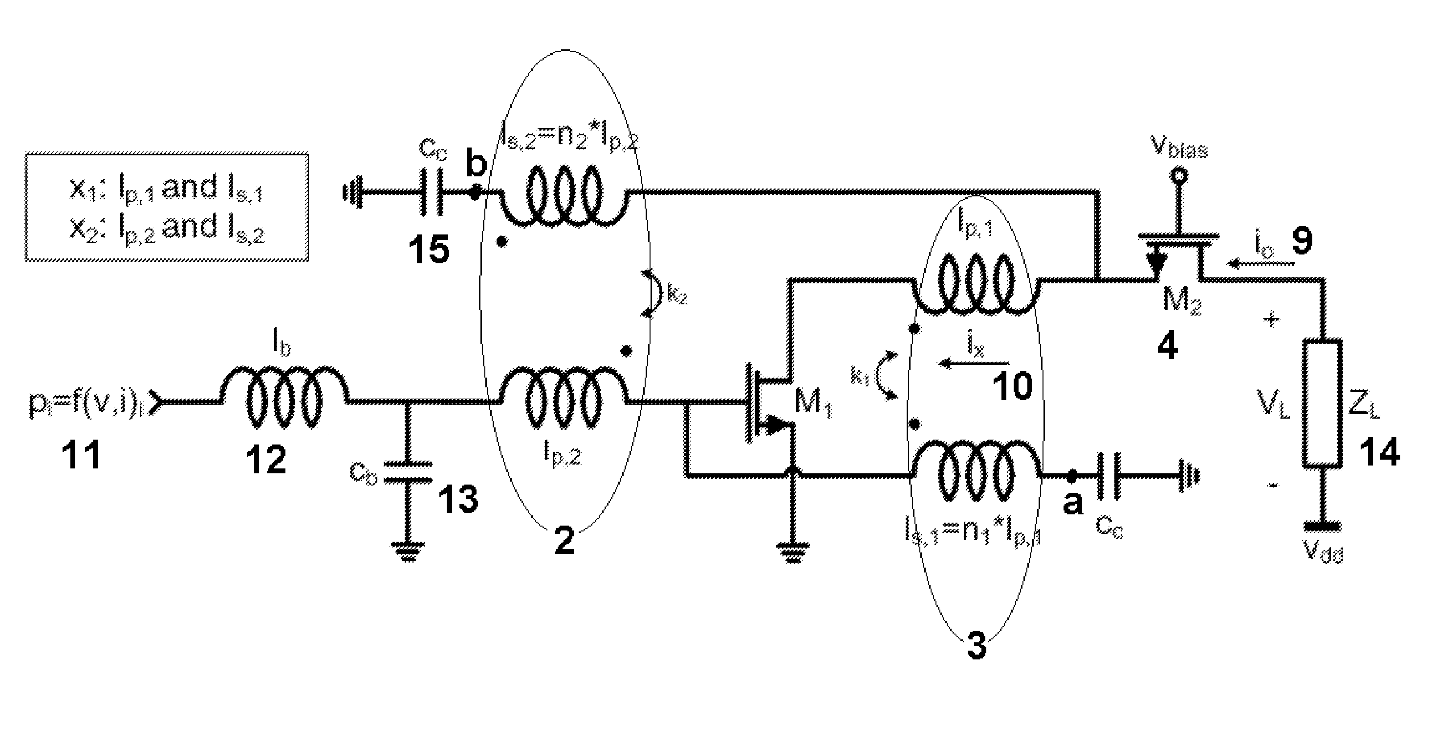
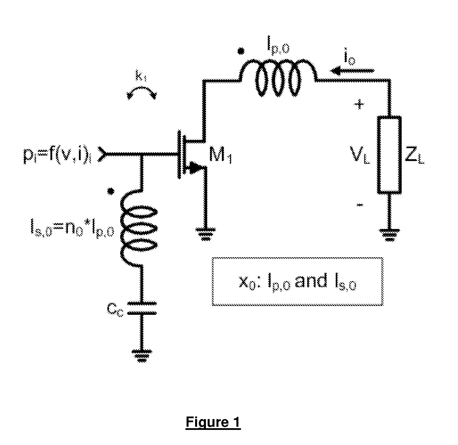
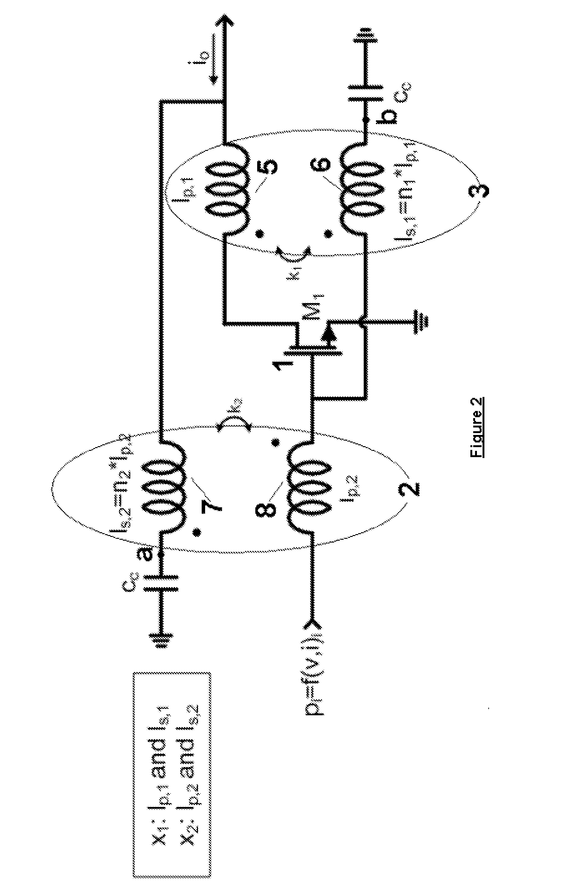
[0031]The present invention will be described with respect to particular embodiments and with reference to certain drawings but the invention is not limited thereto but only by the claims. The drawings described are only schematic and are non-limiting. In the drawings, the size of some of the elements may be exaggerated and not drawn on scale for illustrative purposes. The dimensions and the relative dimensions do not necessarily correspond to actual reductions to practice of the invention.

[0032]Furthermore, the terms first, second, third and the like in the description and in the claims, are used for distinguishing between similar elements and not necessarily for describing a sequential or chronological order. The terms are interchangeable under appropriate circumstances and the embodiments of the invention can operate in other sequences than described or illustrated herein.

[0033]Moreover, the terms top, bottom, over, under and the like in the description and the claims are used fo...


PUM


Abstract

An amplifying circuit arranged for converting an input signal into an amplified output signal comprising: an input node (11) at an input side of said circuit for receiving said input signal (pi); an output node (9) at an output side of said circuit for outputting said amplified output signal (io); a first gain element (M1) connected between said input and output nodes and provided for converting an input voltage taken from said input signal into a current for forming said amplified output signal; a negative feedback loop (3) over said first gain element, said negative feedback loop having first elements (5, 6) arranged for providing input matching; and a positive feedback loop (2) over said first gain element, said positive feedback loop having second elements (7, 8) arranged for providing additional input matching and gain enhancement of said first gain element.

Description

TECHNICAL FIELD[0001]The invention relates to circuits and operation methods for said circuits, for example for amplifying signals, in particular said circuits and methods are suitable for use in narrowband, broad- / (ultra-) wide-band (preferably above 1 GHz) telecommunication systems.BACKGROUND ART[0002]FIG. 1 shows a typical single loop negative feedback amplifier as known in the art. Here the output current (io) is sensed (through the secondary (Is,0) of transformer x0) and applied to the input of M1 (through the primary of the transformer (Ip,0)), thereby resulting in the current-to-current transfer. For the voltage-to-current transfer, the intrinsic transconductance (gm1) of device M1 is used. With these two relationships (i.e., gm1 of M1 and turns ratio of x0), input impedance of the amplifier can be set to the desired value. Since there are only two design variables, the design has as drawback a trade-off between the wanted gain and input impedance.DISCLOSURE OF THE INVENTION[...

Claims


Application Information

Patent Timeline
Patent Type & Authority Applications(United States)
IPC IPC(8): H03F1/34
CPCH03F1/342H03F3/19H03F1/565H03F1/347
Inventor BAGGA, SUMIT
Owner STICHTING IMEC NEDERLAND
Why Eureka
Try Eureka