Laminate, circuit board and semiconductor device

Inactive Publication Date: 2011-06-23
SUMITOMO BAKELITE CO LTD
View PDF10 Cites 11 Cited by
  • Summary
  • Abstract
  • Description
  • Claims
  • Application Information

AI Technical Summary

Benefits of technology

[0029]According to the present invention, a laminate and a circuit board which are reduced in

Problems solved by technology

In response to these requirements, warpage in a printed wiring board becomes a problem.
When warpage occurs in a printed wiring board, in the mounting process, there might be drawbacks such as defective mounting of components, connection failure, sticking at a production

Method used


Image

  • Laminate, circuit board and semiconductor device
  • Laminate, circuit board and semiconductor device
  • Laminate, circuit board and semiconductor device

Examples


example 1

[0118](1) Preparation of Resin Varnish

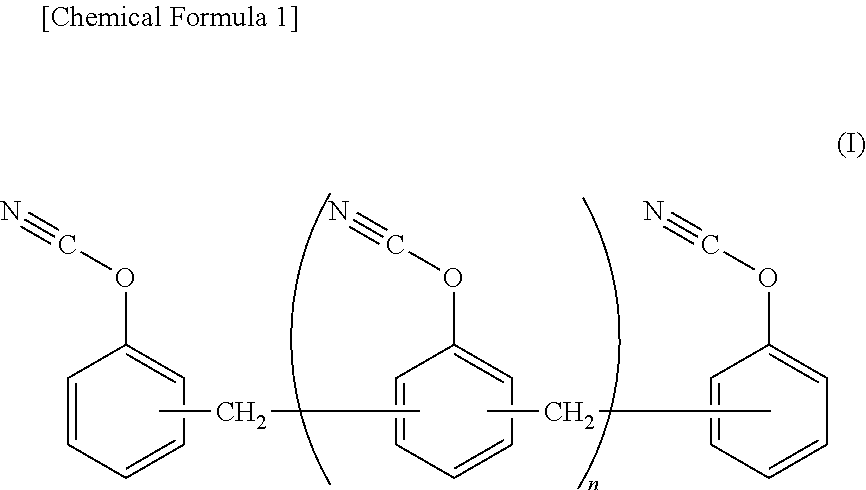
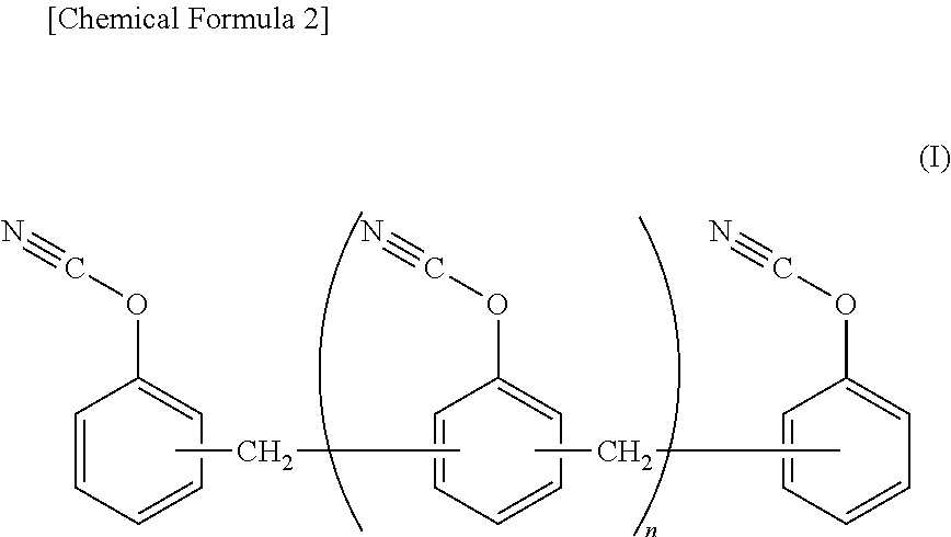
[0119]14.7 parts by weight of a novolac type cyanate resin (Primaset PT-30, manufactured by Lonza Japan, Ltd., weight average molecular weight: about 700), 8 parts by weight of a biphenyldimethylene type epoxy resin (NC-3000H, manufactured by Nippon Kayaku Co., Ltd., epoxy equivalent: 275), 7 parts by weight of a biphenyldimethylene type phenol resin (MEH-7851-3H, manufactured by Meiwa Plastic Industries, Ltd., hydroxyl equivalent: 230), and 0.3 parts by weight of an epoxysilane type coupling agent (A-187, manufactured by GE Toshiba Silicones Co., Ltd.) were dissolved in methyl ethyl ketone at an ambient temperature, and 70 parts by weight of spherical fused silica (SO-25R, manufactured by Admatechs Co., Ltd., average particle size: 0.5 μm) was added to the mixture. The resulting mixture was stirred for 10 minutes using a high-speed stirrer to obtain a resin varnish.

[0120](2) Preparation of Prepreg

[0121]A glass cloth (WEA-2116, manufactured by N...

example 2

[0131]A semiconductor device was obtained in the same manner as in Example 1, except that 19.7 parts by weight of a novolac type cyanate resin (Primaset PT-30, manufactured by Lonza Japan, Ltd., weight average molecular weight: about 700), 11 parts by weight of a biphenyldimethylene type epoxy resin (NC-3000H, manufactured by Nippon Kayaku Co., Ltd., epoxy equivalent: 275), 9 parts by weight of a biphenyldimethylene type phenol resin (MEH-7851-3H, manufactured by Meiwa Plastic Industries, Ltd., hydroxyl equivalent: 230), and 0.3 parts by weight of an epoxysilane type coupling agent (A-187, manufactured by GE Toshiba Silicones Co., Ltd.) were dissolved in methyl ethyl ketone at an ambient temperature, and 60 parts by weight of spherical fused silica (SO-25R, manufactured by Admatechs Co., Ltd., average particle size: 0.5 μm) was used.

example 3

[0132]A semiconductor device was obtained in the same manner as in Example 2, except that an electrolytic copper foil (3EC-M3-VLP, manufactured by Mitsui Kinzoku Co., Ltd.) having a tensile modulus of elasticity at 25° C. of 60 GPa was used.


PUM

PropertyMeasurementUnit
Temperatureaaaaaaaaaa
Fractionaaaaaaaaaa
Fractionaaaaaaaaaa

Abstract

Disclosed is a laminate including an insulating resin layer and a metallic foil formed in contact with the insulating resin layer. The laminate is characterized in that the interface stress between the insulating resin layer and the metallic foil represented by the following formula (1) is not more than 7×10⁴, when the tensile modulus of elasticity (A) of the metallic foil at 25° C. is not less than 30 GPa and not more than 60 GPa, the thermal expansion coefficient (B) of the metallic foil is not less than 10 ppm and not more than 30 ppm, the bending modulus of elasticity (C) of the insulating resin layer at 25° C. is not less than 20 GPa and not more than 35 GPa, and the thermal expansion coefficient (D) of the insulating resin layer in the XY direction from 25° C. to Tg is not less than 5 ppm and not more than 15 ppm,
Interface stress={(B)−(D)}×{(A)−(C)}×{Tg−25 [° C.]}  Formula (1)
wherein, Tg represents the glass transition temperature of the insulating resin layer.

Description

TECHNICAL FIELD[0001]The present invention relates to a laminate, a circuit board and a semiconductor device.BACKGROUND ART[0002]With recent reduction in a size and higher functions of electronic equipment, materials used for printed wiring boards to be mounted thereon require qualities capable of coping with reduction in a size, thinning, high integration, high layer count and high heat resistance. In response to these requirements, warpage in a printed wiring board becomes a problem.[0003]When warpage occurs in a printed wiring board, in the mounting process, there might be drawbacks such as defective mounting of components, connection failure, sticking at a production line and the like. Furthermore, even for a product after mounting, when a printed wiring board is warped at a thermal cycling test, a stress is easily exerted between a printed wiring board and a mounting component, so that disconnection of through holes and disconnection of component connecting portions are easily ...

Claims


Application Information

Patent Timeline
IPC IPC(8): H05K1/18B32B15/08B32B17/04B32B5/00H05K1/00
CPCB32B15/14Y10T428/266B32B27/04B32B27/30B32B27/38H05K1/0353H05K1/09H05K3/022H05K2201/0209H05K2201/0355H05K2201/068H01L2924/0002B32B17/04Y10T428/264Y10T428/12569H01L2924/00Y10T428/31678Y10T428/31529B32B15/08B32B15/092H01L21/00
Inventor TAKAHASHI, AKIHITO
Owner SUMITOMO BAKELITE CO LTD
Why Eureka
Try Eureka