Method and system for specifying system level constraints in a cross-fabric design environment

Inactive Publication Date: 2011-06-23
CADENCE DESIGN SYST INC
View PDF31 Cites 15 Cited by
  • Summary
  • Abstract
  • Description
  • Claims
  • Application Information

AI Technical Summary

Benefits of technology

[0022]An object of embodiments of the invention is to provide a method to eliminate unnecessary physical design iterations during a connection point assignment in the design and manufacture of an electronic system.
[0027]Another object of embodiments of the invention is provide a method to shorten the time required to create an optimum connection point assignment in the design and manufacture of an electronic system.

Problems solved by technology

A design project that is unaware of the impact of other PCB components on the overall placement and routing might lead to suboptimal pin assignment resulting in an increase in the number of layers on a PCB design.
Moreover, the related art approach to the electronic design project may lead to unnecessary iterations at the tail end of the design cycle because the IC design, package design and PCB design teams have to make several iterations to tweak the pin assignment in their respective fabrics.

Method used


Image

  • Method and system for specifying system level constraints in a cross-fabric design environment
  • Method and system for specifying system level constraints in a cross-fabric design environment
  • Method and system for specifying system level constraints in a cross-fabric design environment

Examples


Embodiment Construction

[0050]Reference will now be made in detail to exemplary embodiments which are illustrated in the accompanying drawings. Wherever possible, similar reference numbers will be used to refer to the same or similar parts.

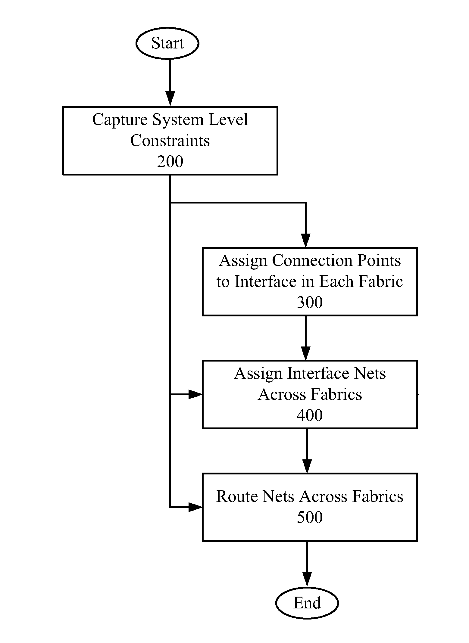
[0051]FIG. 3 shows a chart illustrating an exemplary design flow for an electronic system according to an exemplary embodiment of the invention. Referring to FIG. 3, a method for designing an electronic system includes capturing system level constraints in a first stage 200, assigning connection points to each interface in one or more fabric in a second stage 300, assigning nets between connection points across fabrics in a third stage 400, and routing the nets across the fabrics in a fourth stage 500.

[0052]FIG. 4 shows a flow chart illustrating an exemplary design flow for capturing system level constraints for an electronic system according to an exemplary embodiment of the invention. Referring to FIG. 4, the locations of connection points in each fabric are inputted a...


PUM


Abstract

A method of specifying system level constraints for connecting an interface of an electronic device between first and second fabrics includes specifying one or more first condition relating to a placement of the interface, specifying one or more second condition relating to a connection of a net in the interface between the first and second fabrics, generating one or more first equation expressing the first condition as a function of the location of the connectors, generating one or more second equation expressing the second condition as a function of the location of connectors, generating one or more third equation expressing an optimality criterion for the interface, and outputting the one or more first equation, the one or more second equation and the one or more third equation to a data file in a computer readable format.

Description

BACKGROUND OF THE INVENTION[0001]1. Field of the Invention[0002]The embodiments of invention relate to the automation of the design and manufacturing of electronic systems, more particularly to the method and system for specifying system level constraints in a cross-fabric design environment.[0003]2. Discussion of the Related Art[0004]In general, an electronic system include a plurality of integrated circuit chips (IC) for performing various electronic functions. Each IC includes many electronic components (e.g. transistors, diodes, capacitors, inverters, logic gates, multiplexers, etc.) interconnected in a prescribed manner to respond to input electrical signals and produce other electrical signals according to the desired electronic function performed by the IC. For example, basic electrical components can be combined to form a larger scale component functioning as a memory cell, a multiplexer, or an arithmetic and logic unit (ALU). The various electronic components within the IC ...

Claims


Application Information

Patent Timeline
IPC IPC(8): G06F17/10G06F17/50
CPCG06F17/5077G06F30/394
Inventor BHATTACHARYA, UTPALKOHLI, VIKASBERI, TARUNVERMA, RAHUL
Owner CADENCE DESIGN SYST INC
Why Eureka
Try Eureka