

Drive circuit and display device
- Summary
- Abstract
- Description
- Claims
- Application Information
AI Technical Summary
Benefits of technology
Problems solved by technology
Method used
Image

Examples
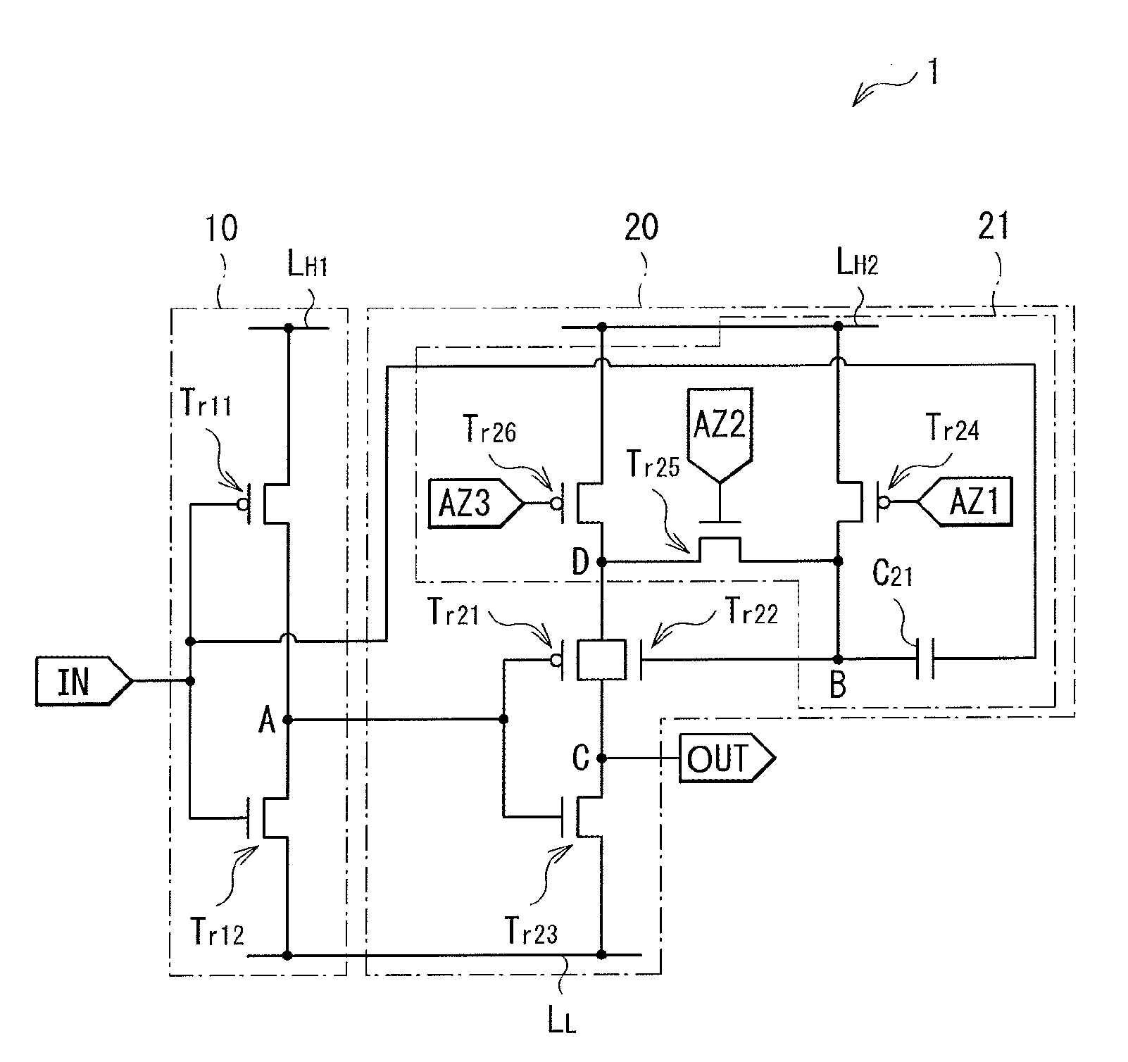
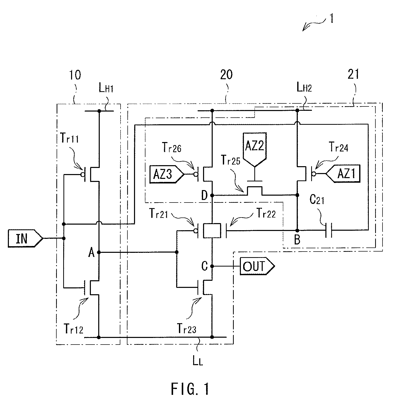
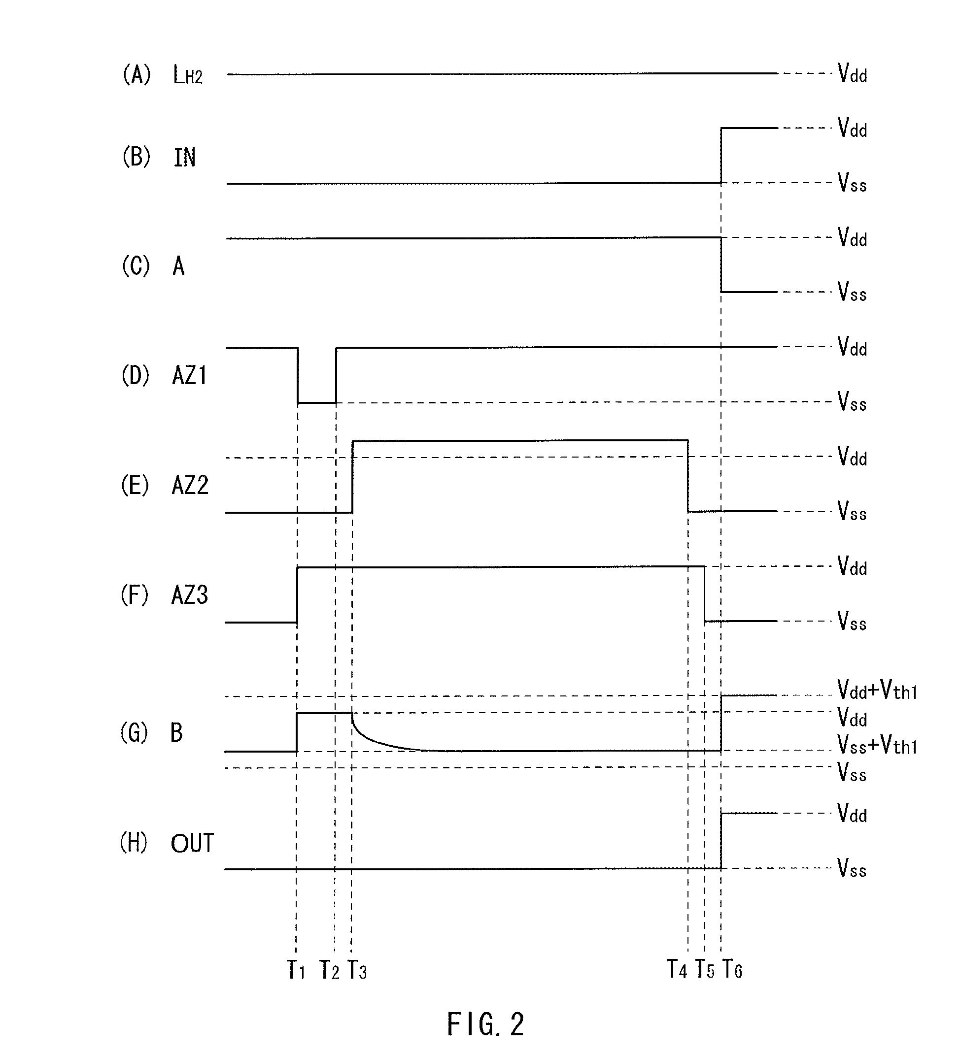
first embodiment
Modification of First Embodiment
[0068]In the above-described embodiment, the transistor Tr24 is a p-channel MOS transistor, and the transistor Tr25 is an n-channel MOS transistor. However, the electro-conductive types of these transistors Tr24 and Tr25 may be all reversed. Specifically, as illustrated in FIG. 3, the transistor Tr24 may be an n-channel MOS transistor, and the transistor Tr25 may be a p-channel MOS transistor. In this case however, as illustrated in FIG. 4, the signal waveforms of the control signals AZ1 and AZ2 are desired to be the inverse of the signal waveforms of the control signals AZ1 and AZ2 illustrated in FIG. 2.
SECOND EMBODIMENT
[0069]Next, a buffer circuit 2 (drive circuit) according to the second embodiment will be described. FIG. 5 illustrates an example of the entire structure of the buffer circuit 2. Like the buffer circuit 1 described above, the buffer circuit 2 outputs, from an output end OUT, a pulse signal approximately in phase with a pulse signal ...
second embodiment
Modification of Second Embodiment
[0080]In the second embodiment, each of the transistors Tr31 and Tr32 is an n-channel MOS transistor, but the electro-conductive types of these transistors Tr31 and Tr32 may be all reversed. Specifically, as illustrated in FIG. 7, each of the transistors Tr31 and Tr32 may be a p-channel MOS transistor. In this case however, as illustrated in, for example, FIG. 8, the signal waveforms of the control signals AZ4 and AZ5 are desired to be the inverse of the signal waveforms of the control signals AZ4 and AZ5 illustrated in FIG. 6.
THIRD EMBODIMENT
[0081]Next, a buffer circuit 3 (drive circuit) according to the third embodiment will be described. FIG. 9 illustrates an example of the entire structure of the buffer circuit 3. Like the buffer circuit 2, the buffer circuit 3 outputs, from an output end OUT, a pulse signal approximately in phase with a pulse signal input into an input end IN. The buffer circuit 3 includes the inverter circuit 10 (input-side in...
third embodiment
Modification of Third Embodiment
[0089]In the third embodiment, the transistor Tr32 is a p-channel MOS transistor, but the electro-conductive type of this transistor Tr32 may be reversed. Specifically, as illustrated in FIG. 11, the transistor Tr32 may be an n-channel MOS transistor. In this case however, as illustrated in FIG. 12, the signal waveform of the control signal AZ5 is desired to be the inverse of the signal waveform of the control signal AZ5 illustrated in FIG. 10.
FOURTH EMBODIMENT
[0090]Next, a buffer circuit 4 (drive circuit) according to the fourth embodiment will be described. FIG. 13 illustrates an example of the entire structure of the buffer circuit 4. Like the above-described buffer circuits 1 and 2, the buffer circuit 4 outputs, from an output end OUT, a pulse signal approximately in phase with a pulse signal input into an input end IN. The buffer circuit 4 includes the inverter circuit 10 (input-side inverter circuit) and an inverter circuit 50 (output-side inve...
PUM
 Abstract
Description
Claims
Application Information