Liquid crystal display unit and method of manufacturing the same
a technology of liquid crystal display unit and liquid crystal, which is applied in the direction of paper/cardboard containers, instruments, transportation and packaging, etc., can solve the problems of complicated manufacturing steps, and achieve the effects of easy retention of favorable display characteristics, increased response rate according to electric field between electrodes, and favorable display characteristics
- Summary
- Abstract
- Description
- Claims
- Application Information
AI Technical Summary
Benefits of technology
Problems solved by technology
Method used
Image
Examples
first embodiment
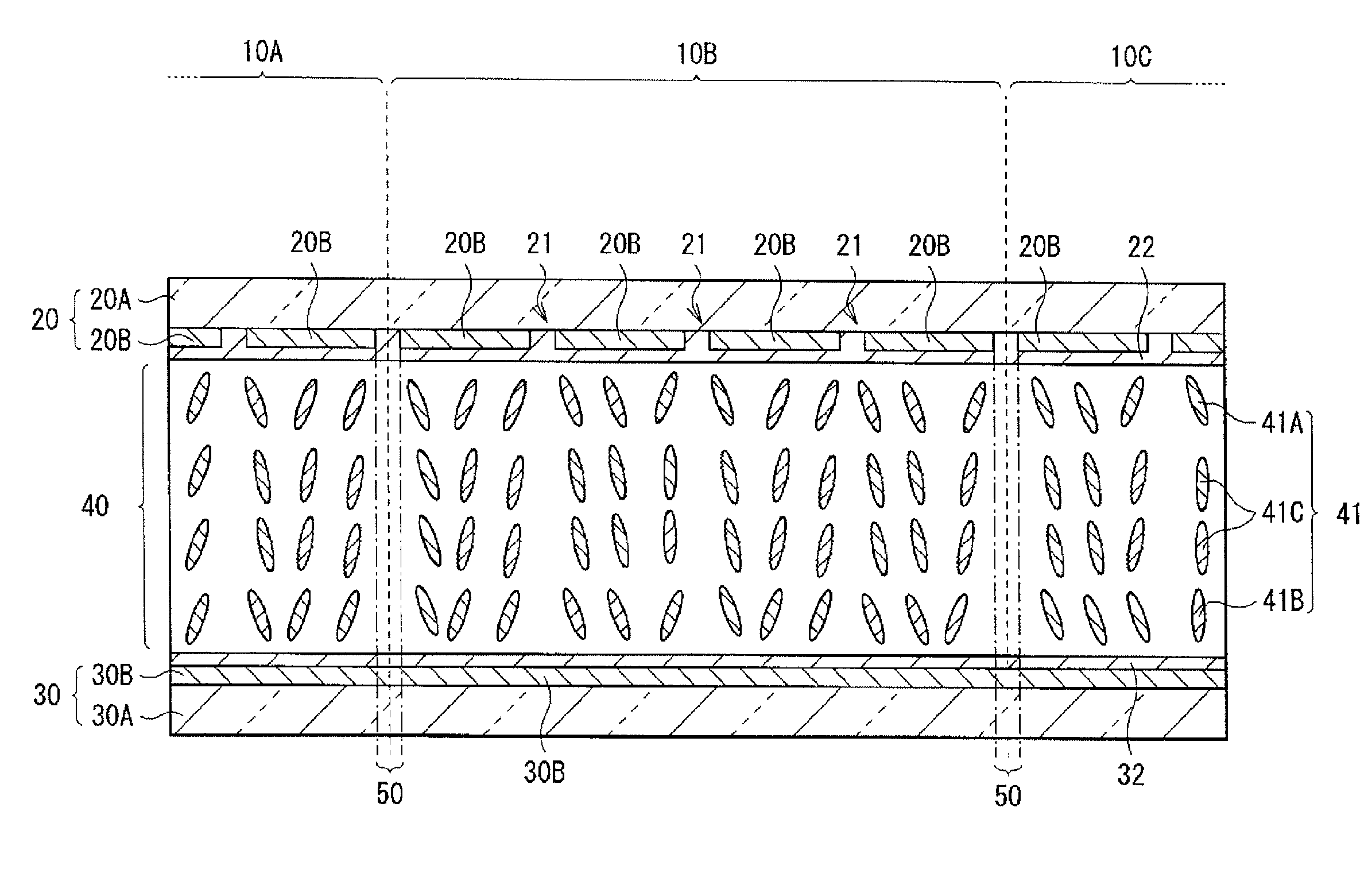
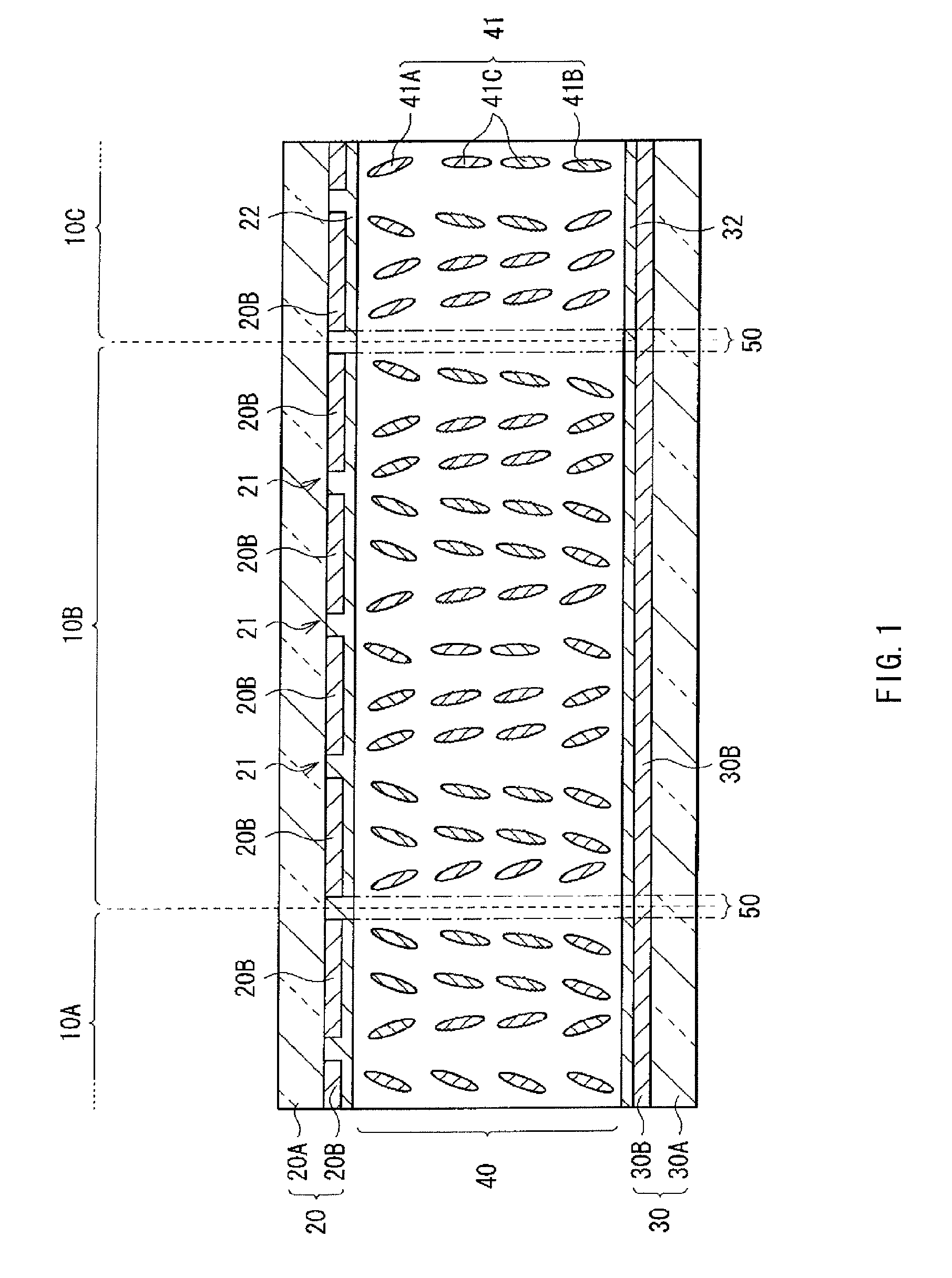
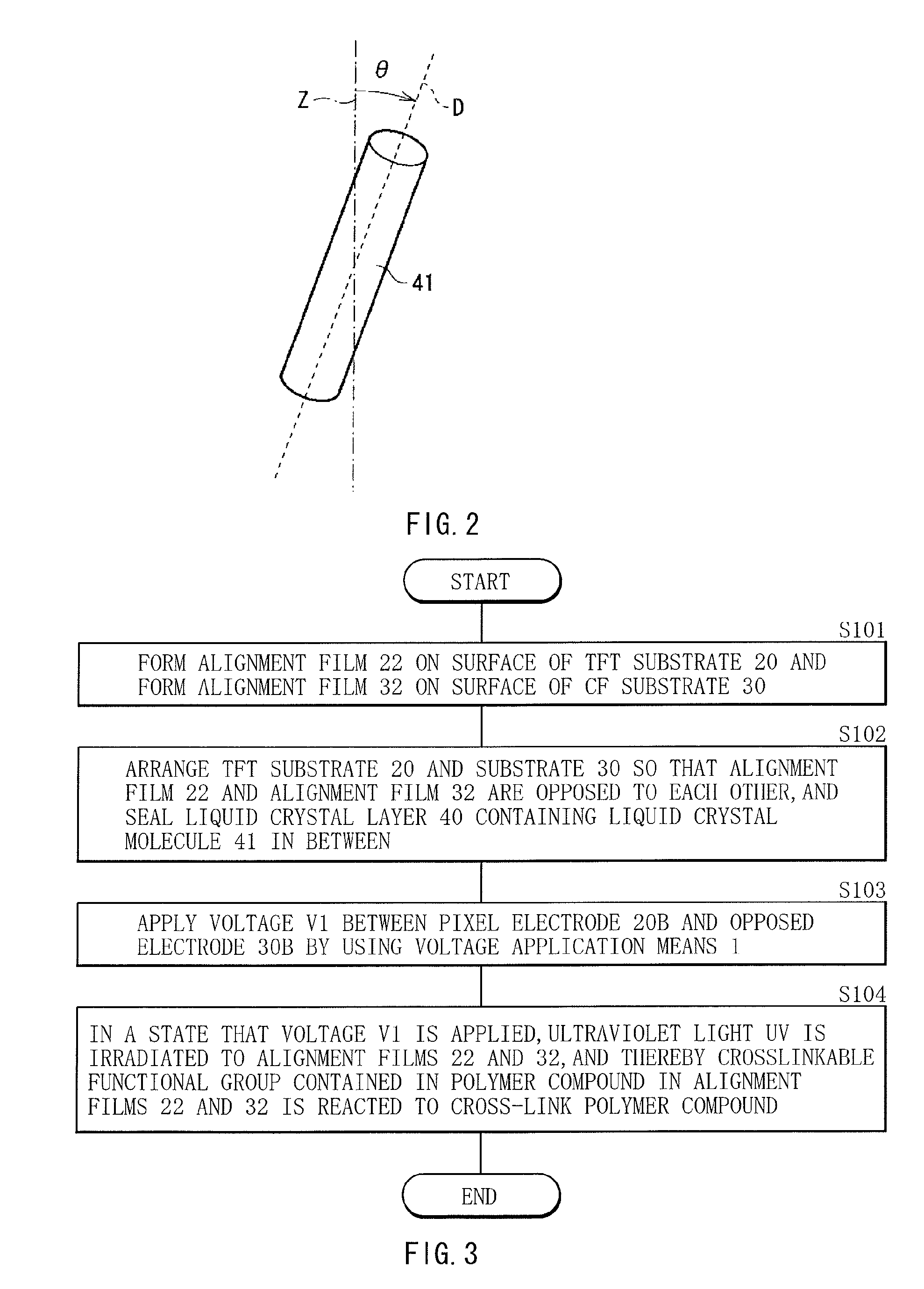
[0072]A first embodiment relates to the VA mode liquid crystal display unit (or liquid crystal display device) according to the first aspect of the present invention, and methods of manufacturing a liquid crystal display units (or liquid crystal display devices) according to the first aspect of the present invention and the third aspect of the present invention. In the first embodiment, the alignment films 22 and 32 contain one or more polymer compounds having a cross-linking structure in a side chain (compound after alignment process). Liquid crystal molecules are given with pretilt by the cross-linked compound. In this case, the compound after alignment process is generated by forming the alignment films 22 and 32 containing one or more polymer compounds (compound before alignment process) having a main chain and a side chain, providing the liquid crystal layer 40, and then bridging the polymer compound; or radiating energy line to the polymer compound; or more specifically, by re...
second embodiment
[0141]A second embodiment is a modified embodiment of the first embodiment. In the first embodiment, the description has been given of the liquid crystal display unit (liquid crystal display device) in which the alignment films 22 and 32 are formed so that the pretilt θ1 and the pretilt θ2 of the liquid crystal molecules 41A and 41B located in the vicinity of the alignment films 22 and 32 are almost the same. In the second embodiment, the pretilt θ1 value is different from the pretilt θ2 value.
[0142]Specifically, in the second embodiment, first, the TFT substrate 20 having the alignment film 22 and the CF substrate 30 having the alignment film 32 are formed in the same manner as that of the foregoing step S101. Next, for example, an ultraviolet absorber is contained in the liquid crystal layer 40 and is sealed. Subsequently, a predetermined voltage is applied between the pixel electrode 20B and the opposed electrode 30B, ultraviolet is irradiated from the TFT substrate 20 side, and ...
third embodiment
[0143]A third embodiment is a modified embodiment of the first embodiment and the second embodiment. FIG. 10 illustrates a schematic partial cross sectional view of a liquid crystal display unit (liquid crystal display device) according to the third embodiment. Differently from the first embodiment, in the third embodiment, the alignment film 22 does not contain the compound after alignment process. That is, in the third embodiment, the pretilt θ2 of the liquid crystal molecules 41B located in the vicinity of the alignment film 32 has a higher value than 0 deg, while the pretilt θ1 of the liquid crystal molecules 41A located in the vicinity of the alignment film 22 is 0 deg.
[0144]In this case, the alignment film 22 includes, for example, the foregoing other vertical aligner.
[0145]The liquid crystal display unit (liquid crystal display device) of the third embodiment is able to be manufactured by using the foregoing other vertical aligner instead of the compound before alignment proc...
PUM
| Property | Measurement | Unit |
|---|---|---|
| surface roughness | aaaaa | aaaaa |
| surface roughness Ra | aaaaa | aaaaa |
| wavelength | aaaaa | aaaaa |
Abstract
Description
Claims
Application Information


