Schottky diode with low reverse leakage current and low forward voltage drop

Inactive Publication Date: 2011-07-07
PYNMAX TECH
View PDF8 Cites 0 Cited by
  • Summary
  • Abstract
  • Description
  • Claims
  • Application Information

AI Technical Summary

Benefits of technology

[0008]An objective of the invention is to provide a Schottky diode that keeps the advantages of high-speed operations and low forward voltage drop under a forward current and suppresses the leakage current under a reverse current.
[0012]In the above-mentioned structure, depletion regions form at the junction between the second conductive material regions and the first conductive material semiconductor substrate. The depletion regions can reduce the leakage current area when the Schottky diode operates under a reverse voltage. Therefore, it can reduce the reverse leakage current and the forward voltage drop.

Problems solved by technology

When the current Schottky diode is imposed with a reverse voltage, it often has a large leakage current that limits its applications.
Moreover, when imposed with a forward current load, it cannot have the advantage of relatively low forward voltage drop under both high and low current densities.

Method used


Image

  • Schottky diode with low reverse leakage current and low forward voltage drop
  • Schottky diode with low reverse leakage current and low forward voltage drop
  • Schottky diode with low reverse leakage current and low forward voltage drop

Examples


first embodiment

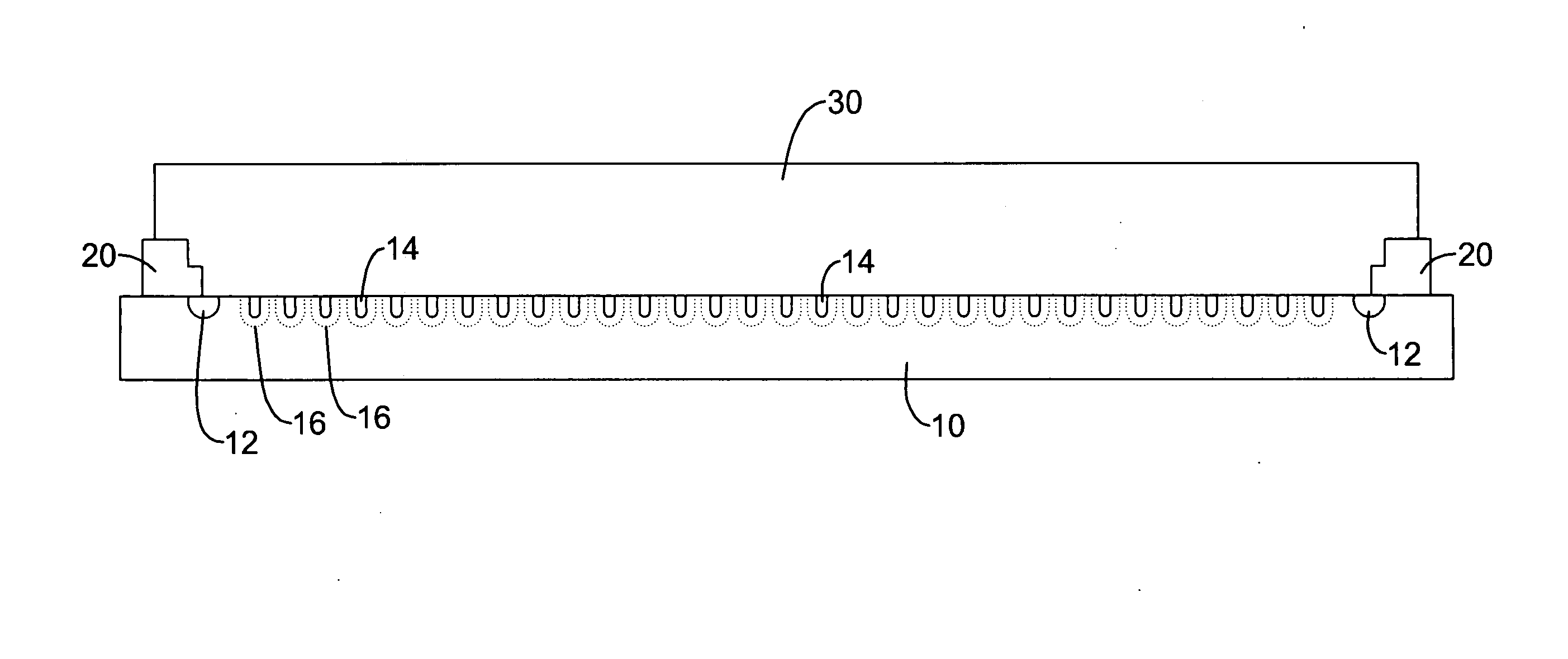
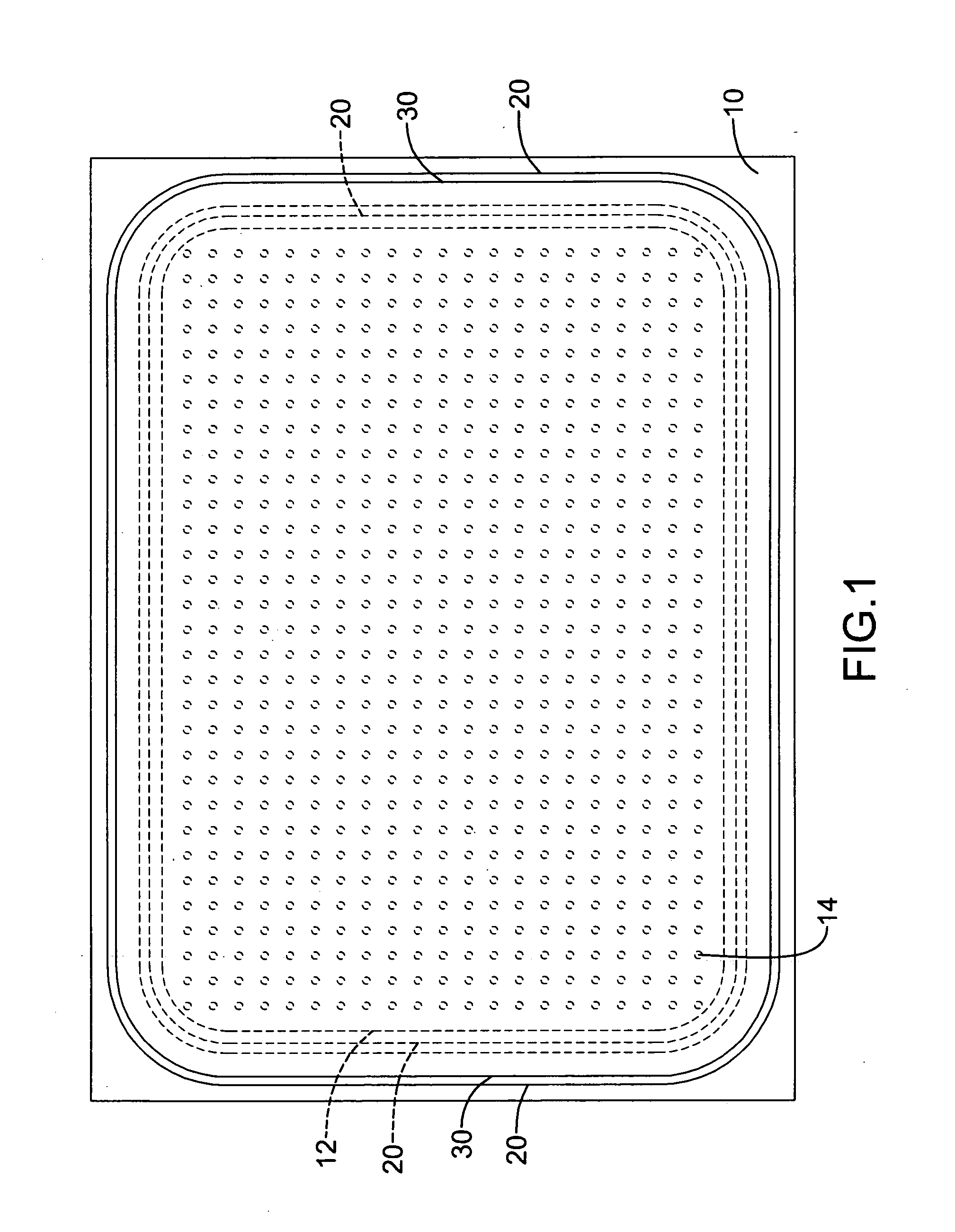
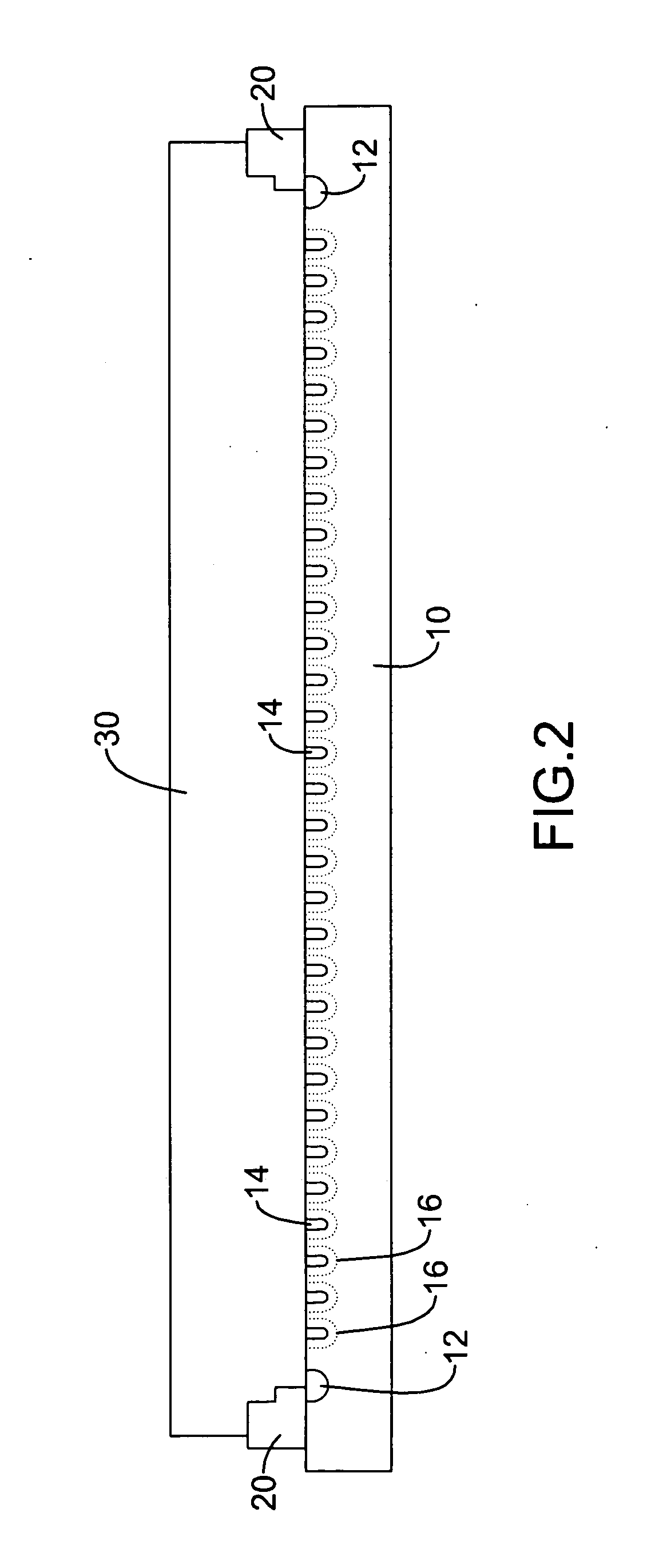
[0022]With reference to FIGS. 1 and 2, a first embodiment in accordance with the present invention comprises a first conductive material semiconductor substrate (10), an oxide layer (20), and a metal layer (30).

[0023]The first conductive material semiconductor substrate (10) is a substrate made of a first conductive material semiconductor material, such as an N-type substrate made of group-V elements As and P. The surrounding of the first conductive material semiconductor substrate (10) is formed with an annular protection ring (12). The annular protection ring (12) is made of the second conductive material and formed in the first conductive material semiconductor substrate (10). The area enclosed by the protection ring (12) is defined as an active area. Multiple second conductive material regions (14) are formed in the active area of the first conductive material semiconductor substrate (10). The second conductive material regions (14) can dot-shaped. In this embodiment, the dot-sh...

second embodiment

[0028]With reference to FIGS. 3 and 4 for the invention, the second conductive material regions (14) are also dot-shaped and distributed in the first conductive material semiconductor substrate (10). However, they are not arranged in an array configuration, but alternating instead. That is, the second conductive material region (14) in each row is not in alignment with its most adjacent second conductive material regions (14) on the next row or previous row. Take any second conductive material region (14) along with its most adjacent two second conductive material regions (14), one obtains an equilateral triangle (40). The depletion regions (16) produced in such an arrangement cover a larger area and thus increase the suppression of reverse leakage current. This is because the gap between adjacent depletion regions (16) can be effectively reduced.

third embodiment

[0029]With reference to FIG. 6 for the invention, in comparison with the above-mentioned embodiments, the second conductive material regions (14) are arranged in lines here. The lines are arranged in two parallel sets that cross each other to form a mesh. In this embodiment, the two sets of second conductive material regions (14) are perpendicular to each other.

[0030]With reference to FIG. 7 for a plan view of a fourth embodiment it differs from the third embodiment in that the two sets of second conductive material regions (14) cross each other at an oblique angle. The region enclosed by the second conductive material regions (14) is an equilateral rhombus. The equilateral rhombus can be considered as the combination of two equilateral triangles. Therefore, the equilateral rhombus has two opposite 60-degree interior angles and two opposite 120-degree interior angles. Such an oblique arrangement can provide a depletion region covering a larger area.

[0031]In summary, the invention fo...


PUM


Abstract

A Schottky diode structure with low reverse leakage current and low forward voltage drop has a first conductive material semiconductor substrate combined with a metal layer. An oxide layer is formed around the edge of the combined conductive material semiconductor substrate and the metal layer. A plurality of dot-shaped or line-shaped second conductive material regions are formed on the surface of the first conductive material semiconductor substrate connecting to the metal layer. The second conductive material regions form depletion regions in the first conductive material semiconductor substrate. The depletion regions can reduce the leakage current area of the Schottky diode, thereby reducing the reverse leakage current and the forward voltage drop. When the first conductive material is a P-type semiconductor, the second conductive material is an N-type semiconductor. When the first conductive material is an N-type semiconductor, the second conductive material is a P-type semiconductor.

Description

BACKGROUND OF THE INVENTION[0001]1. Field of the Invention[0002]The invention relates to a Schottky diode and, in particular, to a Schottky diode that can reduce the reverse leakage current and has a low forward voltage drop.[0003]2. Description of Related Art[0004]With reference to FIG. 8, the characteristic curve A in the drawing is depicted for a normal P-N diode. The other characteristic curve B is depicted for a normal Schottky diode. When the current imposed on the diode is a forward current, it is seen that the forward voltage drop of the P-N diode is larger than that of the Schottky diode when the forward current is small. However, as the forward current increases, the increased forward voltage per unit of the increased current for the P-N type diode is smaller than that of the Schottky diode. In the large forward current region, the forward voltage drop of the Schottky diode is similar to a resistor and increases rapidly. Therefore, its forward voltage drop is much larger t...

Claims


Application Information

Patent Timeline
IPC IPC(8): H01L29/872H01L29/06
CPCH01L29/872H01L29/0692
Inventor TUNG, CHIUN-YENCHEN, KUN-HSIENWANG, KAI-YINGWENG, HUNG TASHEN, YI-CHEN
Owner PYNMAX TECH
Why Eureka
Try Eureka