
Lithographic apparatus, device manufacturing method, and method of applying a pattern to a substrate

a technology of lithographic apparatus and manufacturing method, which is applied in the direction of measurement devices, optical devices, instruments, etc., can solve the problem of limiting the throughput of the apparatus (wafers per hour), and achieve the effect of reducing the delay in the level mapping process, saving time, and increasing the throughput of the lithographic apparatus

Inactive Publication Date: 2011-07-07
ASML NETHERLANDS BV
View PDF17 Cites 22 Cited by
  • Summary
  • Abstract
  • Description
  • Claims
  • Application Information

AI Technical Summary

Benefits of technology

The invention provides a lithographic apparatus with a level sensor that uses optical scanning to measure surface level variations on a substrate. This eliminates the need for mechanical movement between the level sensor and the substrate, reducing delay in the level mapping process and increasing throughput of the lithographic apparatus. The level sensor can have one or more moving optical elements that synchronize with each other during scanning. The invention also provides a method of measuring level variations across a substrate in a lithographic apparatus, which can be used in other fields such as metrology.

Problems solved by technology

In the example of patterning by optical projection, for example, level variations will disturb the focusing of the projected pattern, and hence the contrast between exposed and unexposed parts of the resist.
This sweeping movement takes time in the measuring step, which inevitably limits the throughput of the apparatus (wafers per hour).

Method used


Image

  • Lithographic apparatus, device manufacturing method, and method of applying a pattern to a substrate
  • Lithographic apparatus, device manufacturing method, and method of applying a pattern to a substrate
  • Lithographic apparatus, device manufacturing method, and method of applying a pattern to a substrate

Examples


Embodiment Construction

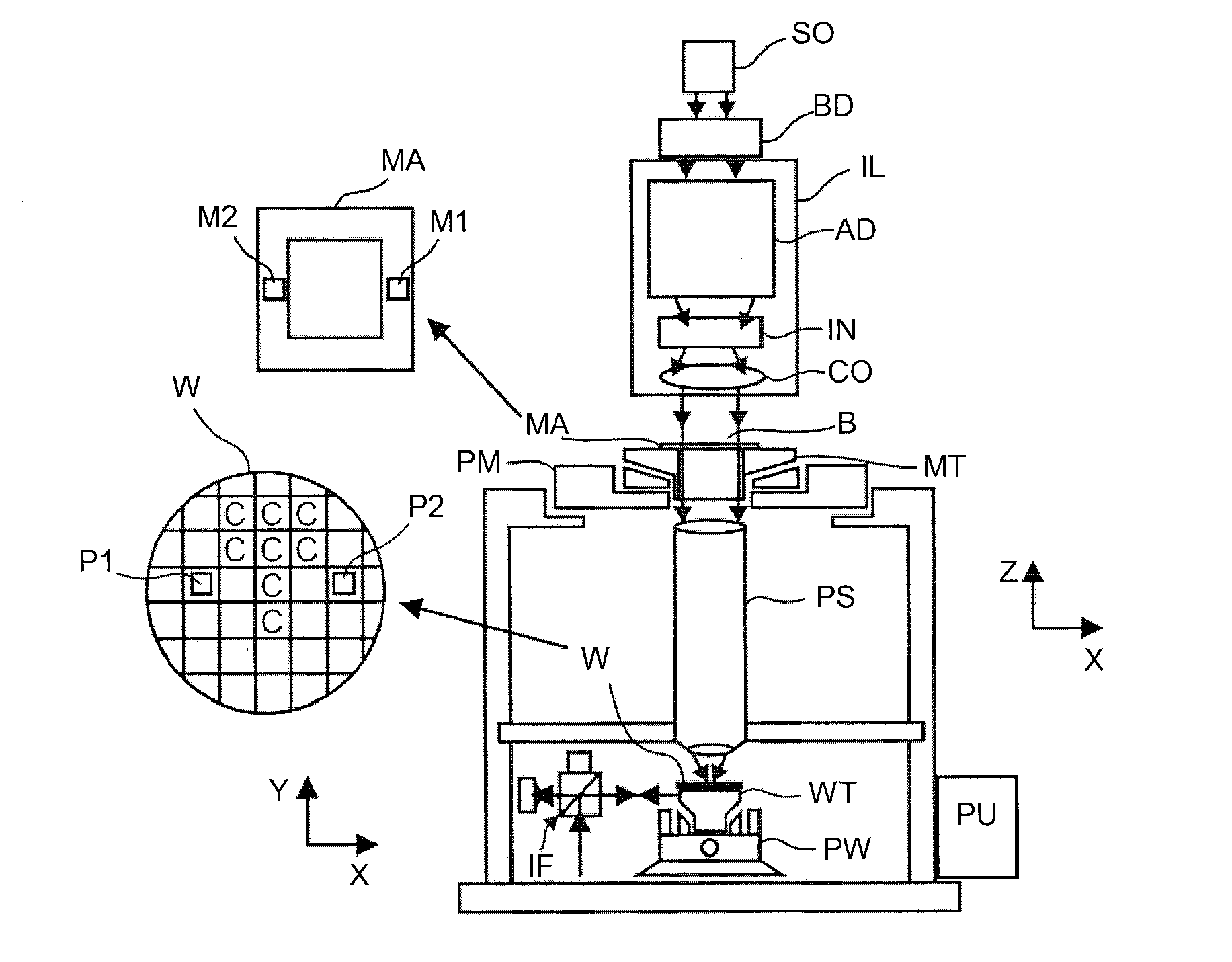
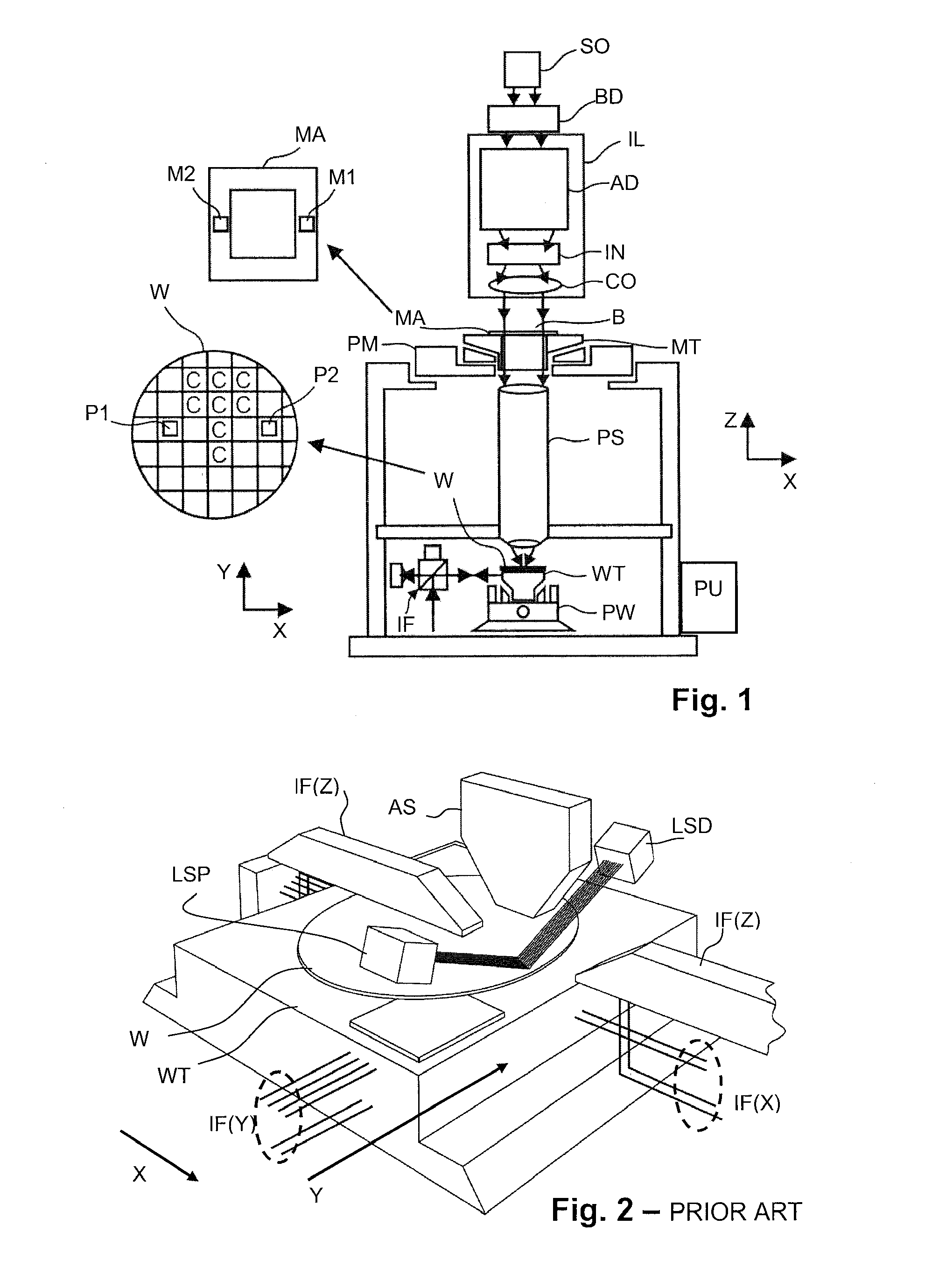
[0036]FIG. 1 schematically depicts a lithographic apparatus according to one embodiment of the invention. The apparatus comprises:

[0037]an illumination system (illuminator) IL configured to condition a radiation beam B (e.g. UV radiation or EUV radiation).

[0038]a support structure (e.g. a mask table) MT constructed to support a patterning device (e.g. a mask) MA and connected to a first positioner PM configured to accurately position the patterning device in accordance with certain parameters;

[0039]a substrate table (e.g. a wafer table) WT constructed to hold a substrate (e.g. a resist-coated wafer) W and connected to a second positioner PW configured to accurately position the substrate in accordance with certain parameters; and

[0040]a projection system (e.g. a refractive projection lens system) PS configured to project a pattern imparted to the radiation beam B by patterning device MA onto a target portion C (e.g. comprising one or more dies) of the substrate W.

[0041]The illuminat...


PUM


Abstract

A lithographic apparatus includes a patterning subsystem for transferring a pattern from a patterning device onto a substrate controlled in accordance with recorded measurements of level variations across a surface of the substrate. A level sensor is provided for projecting a level sensing beam of radiation to reflect from a location on the substrate surface and for detecting the reflected sensing beam to record the surface level at said location. The level sensor incorporates at least one moving optical element to scan the substrate surface by optical movement in at least one dimension to obtain measurements of surface level at different locations without mechanical movement between the level sensor and the substrate. Optical path length equalization measures may be employed, using shaped reflectors and / or additional moving mirrors, to avoid focus variation during the scan.

Description

[0001]This application claims priority and benefit under 35 U.S.C. §119(e) to U.S. Provisional Patent Application No. 61 / 289,855, entitled “Lithographic Apparatus, Device Manufacturing Method, and Method Of Applying A Pattern To A Substrate,” filed on Dec. 23, 2009. The content of that application is incorporated herein in its entirety by reference.FIELD[0002]The present invention relates to a lithographic apparatus and a method for manufacturing a device. The invention relates in particular to methods and devices for measuring surface level variations across a substrate, prior to applying a pattern from a patterning device onto a substrate, though the invention may also be applied for measuring surface level variations on other types of target for other purposes. The invention further relates to a computer program product for controlling a lithographic apparatus to implement steps of such methods.BACKGROUND[0003]A lithographic apparatus is a machine that applies a desired pattern o...

Claims


Application Information

Patent Timeline
Patent Type & Authority Applications(United States)
IPC IPC(8): G03B27/42G01B11/24
CPCG03F9/7034G03F9/7003
Inventor STAALS, FRANKVAN DE KERKHOF, MARCUS ADRIANUS
Owner ASML NETHERLANDS BV
Learn More