Inspection guided overlay metrology

a metrology and overlay technology, applied in the direction of mechanical roughness/irregularity measurement, semiconductor/solid-state device testing/measurement, instruments, etc., can solve the problems of time-consuming and complex setup of two different tools, failure to detect defects of decreasing size, and failure to properly function devices

Active Publication Date: 2011-07-14
KLA TENCOR TECH CORP
View PDF16 Cites 112 Cited by
  • Summary
  • Abstract
  • Description
  • Claims
  • Application Information

AI Technical Summary

Benefits of technology

A method for inspection guided overlay metrology is disclosed. In one aspect, the method for inspection guided overlay metrology may include, but is not limited to, performing a pattern search in order to identify one or more instances of a predetermined pattern on a semiconductor wafer, generating a care area for each of the one or more instances of the predetermined pattern on the semiconductor wafer, identifying one or more defects within each of the one or more generated care areas by performing an inspection scan of each of the one or more generated care areas, wherein the inspection scan includes a low-threshold inspection scan or a high sensitivity inspection scan, identifying one or more overlay sites of at least some of the one or more instances of the predetermined pattern of the semiconductor wafer having a measured overlay error larger than a selected overlay specification utilizing a defect inspection technique, comparing location data of the one or more identified defects of a generated care area to location data of the one or more identified overlay sites within the generated care area in order to identify one or more locations wherein the one or more defects are proximate to the one or more identified overlay sites, and generating a metrology sampling plan based on the identified one or more locations wherein the one or more defects are proximate to the one or more identified overlay sites.

Problems solved by technology

For instance, as the dimensions of semiconductor devices decrease, detection of defects of decreasing size has become necessary since even relatively small defects may cause unwanted aberrations in the semiconductor devices.
The differences detected between the two device areas can either be a defect, which can cause a device to function improperly, or a nuisance, which will not affect system operations.
Setting up two recipes for two different tools is time consuming and complex.
If the two layers or patterns are not properly formed, then the structure on one layer or pattern tends to be offset or misaligned relative to the structure on the other layer or pattern.
Overlay error is the misalignment between any of the patterns used at different stages of semiconductor integrated circuit manufacturing.
Conventionally, understanding of the variation across die and wafer are limited to the fixed sampling and hence overlay error is detected only for the known selected sites.
There are, however, a number of disadvantages to using metrology processes and tools to measure one or more characteristics of a wafer for process monitoring and control applications.
For example, most metrology tools are relatively slow, particularly compared to inspection systems.
As such, using metrology measurements performed at one location or a limited number of locations on a wafer may not provide sufficient information about the characteristic(s) of the wafers such that the process can be accurately monitored and controlled.
Therefore, the sampling plan of the metrology process can significantly affect the meaningfulness and usefulness of the metrology results.
There are, however, a number of disadvantages to currently used metrology sampling plans.
Therefore, one of the disadvantages of currently used metrology sampling plans is that the fixed sites that are sampled during metrology may not be sensitive to subtle variations in the process.

Method used


Image

  • Inspection guided overlay metrology
  • Inspection guided overlay metrology
  • Inspection guided overlay metrology

Examples


Embodiment Construction

Reference will now be made in detail to the subject matter disclosed, which is illustrated in the accompanying drawings.

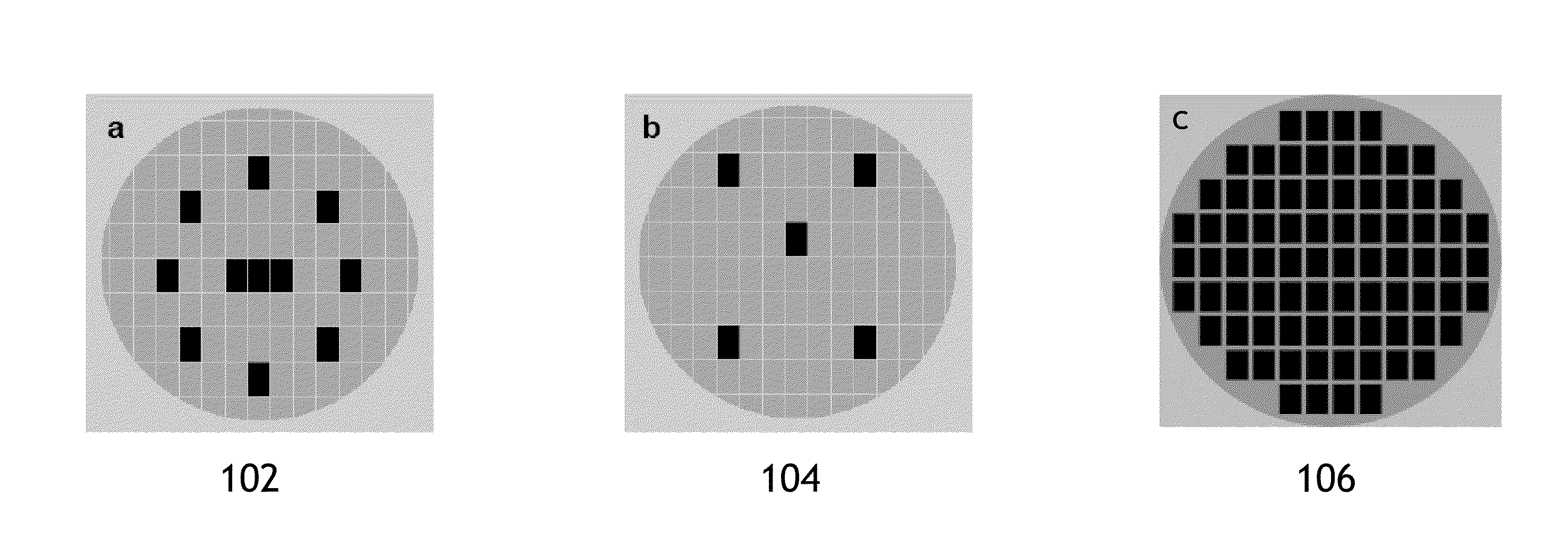
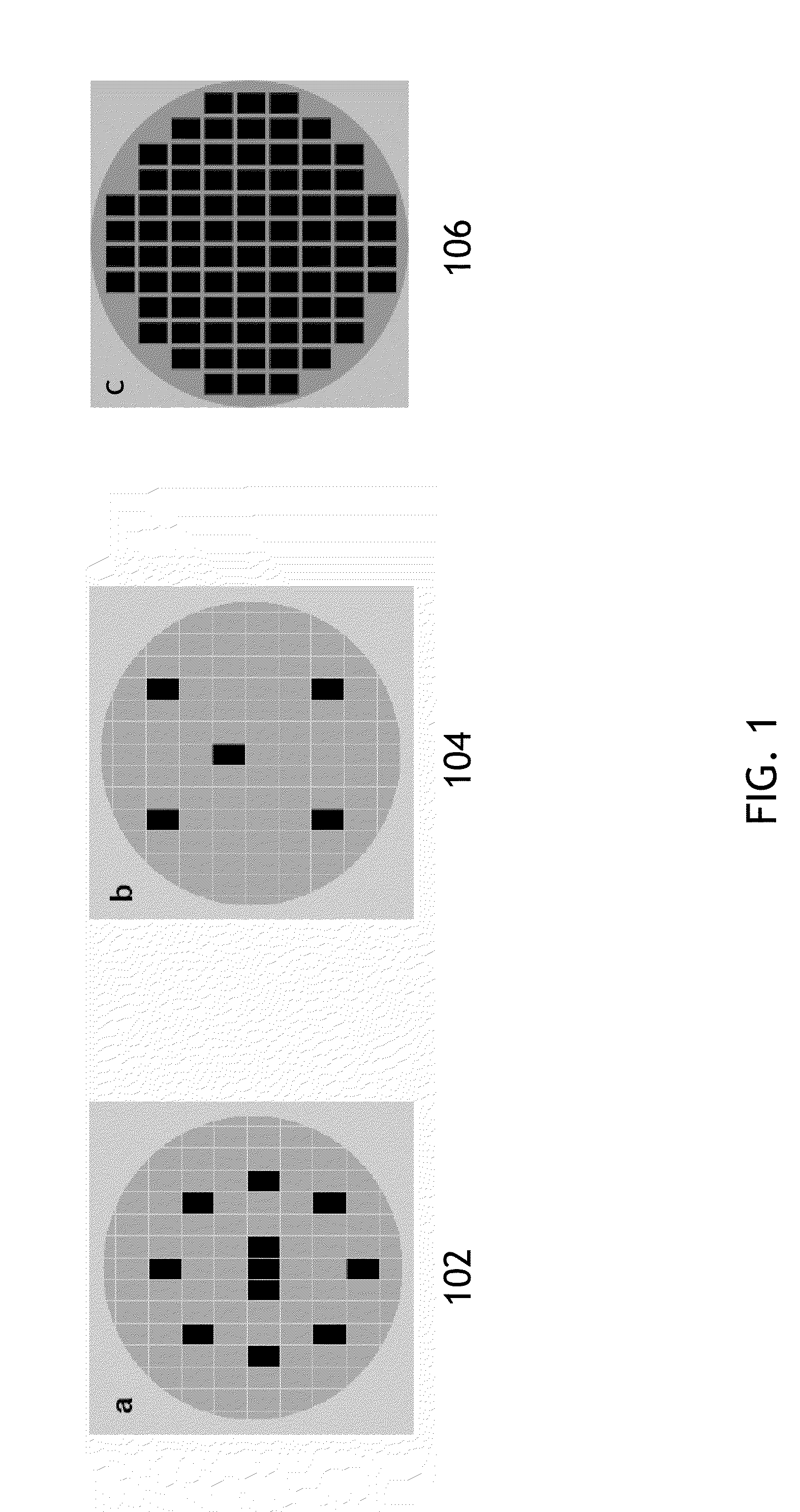
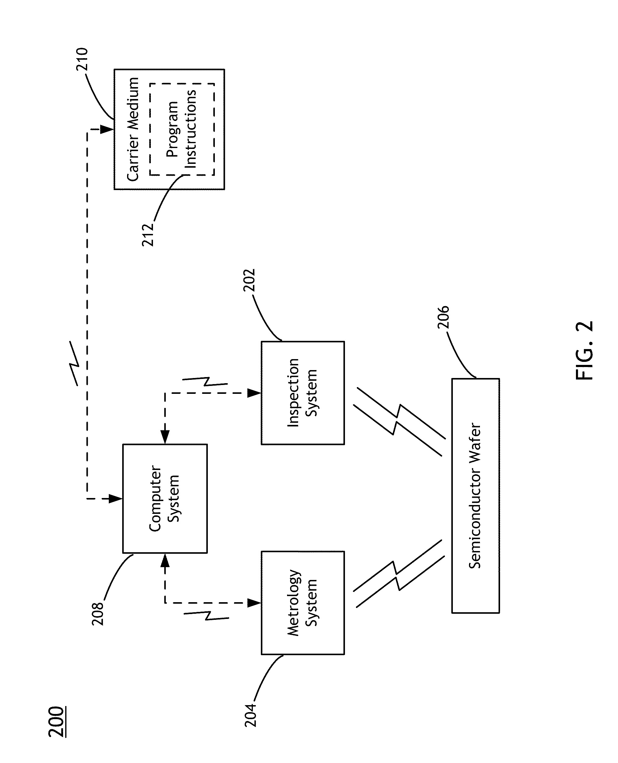
Referring generally to FIGS. 1 through 4B, a method and system for inspection driven overlay metrology is described in accordance with the present disclosure. Employing a combined defect inspection and overlay metrology technique may aid in optimizing overall semiconductor defect and overlay measurement sensitivity and sampling coverage on a semiconductor wafers. Conventionally overlay sampling is carried out at only fixed locations of a semiconductor wafer. The present invention is directed at providing a method and system for providing overlay sampling at dynamic locations of the semiconductor wafer, thereby extending the aerial extent of overlay error and abnormality detection. One aspect of the present invention is the use of an inspection signal associated with detected wafer anomalies as a mechanism for initially detecting overlay metrology sites displaying o...


PUM

PropertyMeasurementUnit
sizeaaaaaaaaaa
areaaaaaaaaaaa
defect inspectionaaaaaaaaaa

Abstract

Inspection guided overlay metrology may include performing a pattern search in order to identify a predetermined pattern on a semiconductor wafer, generating a care area for all instances of the predetermined pattern on the semiconductor wafer, identifying defects within generated care areas by performing an inspection scan of each of the generated care areas, wherein the inspection scan includes a low-threshold or a high sensitivity inspection scan, identifying overlay sites of the predetermined pattern of the semiconductor wafer having a measured overlay error larger than a selected overlay specification utilizing a defect inspection technique, comparing location data of the identified defects of a generated care area to location data of the identified overlay sites within the generated care area in order to identify one or more locations wherein the defects are proximate to the identified overlay sites, and generating a metrology sampling plan based on the identified locations.

Description

CROSS-REFERENCE TO RELATED APPLICATIONThe present application is related to and claims the benefit of the earliest available effective filing date(s) from the following listed application(s) (the “Related Applications”) (e.g., claims earliest available priority dates for other than provisional patent applications or claims benefits under 35 USC §119(e) for provisional patent applications, for any and all parent, grandparent, great-grandparent, etc. applications of the Related Application(s)).TECHNICAL FIELDThe present invention generally relates to a methods and systems for generating a metrology sampling plan, and more particularly to inspection guided overlay metrology of a semiconductor wafer.BACKGROUNDFabricating semiconductor devices such as logic and memory devices typically includes processing a substrate such as a semiconductor wafer using a large number of semiconductor fabrication processes to form various features and multiple levels of the semiconductor devices. For exam...

Claims


Application Information

Patent Timeline
Patent Type & Authority Applications(United States)
IPC IPC(8): G01N21/00
CPCG01N21/9501G01N21/95607G01N2021/8822G03F7/70633G03F7/7065H01L2924/0002H01L22/12H01L2924/00H01L22/00
Inventor CHANG, ELLISWIDMANN, AMIRPARK, ALLEN
Owner KLA TENCOR TECH CORP
Why Eureka
Try Eureka