Semiconductor device and manufacturing method thereof

a technology of semiconductor devices and manufacturing methods, applied in semiconductor devices, semiconductor/solid-state device testing/measurement, electrical equipment, etc., can solve the problems of extending the flow time, affecting the isolation capacity of the substrate, and the above-described method requires much processing time and cost, so as to enhance the isolation capacity, and reduce the effect of air gap portions

Active Publication Date: 2011-07-21
RENESAS ELECTRONICS CORP
View PDF4 Cites 30 Cited by
  • Summary
  • Abstract
  • Description
  • Claims
  • Application Information

AI Technical Summary

Benefits of technology

[0011]In the present example, a trench is formed after completion of the element so that no resist penetrates in the trench during formation of the element. It is therefore possible to realize a semiconductor device not requiring to ensure a high burying property in a simple process, and a manufacturing method of the

Problems solved by technology

This requires twice deposition of insulating films and anisotropic etching for widening the upper end portion of the opening, leading to extension of a flow time.
As a result, the above-described method needs much processing time and cost.
In addition, when the trench has an air gap therein,

Method used


Image

  • Semiconductor device and manufacturing method thereof
  • Semiconductor device and manufacturing method thereof
  • Semiconductor device and manufacturing method thereof

Examples


embodiment 1

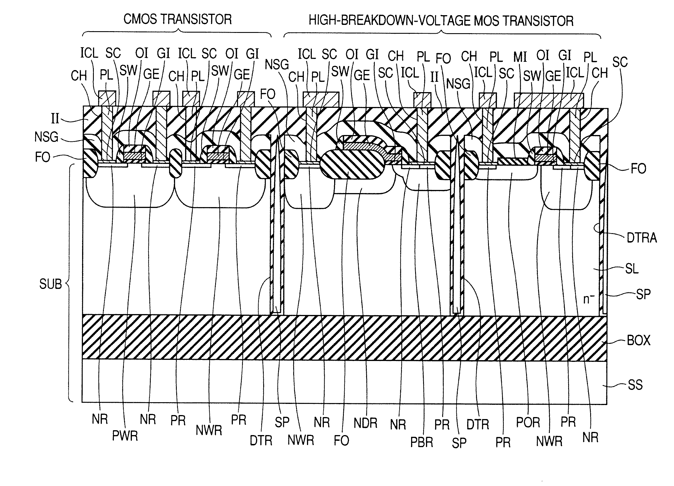
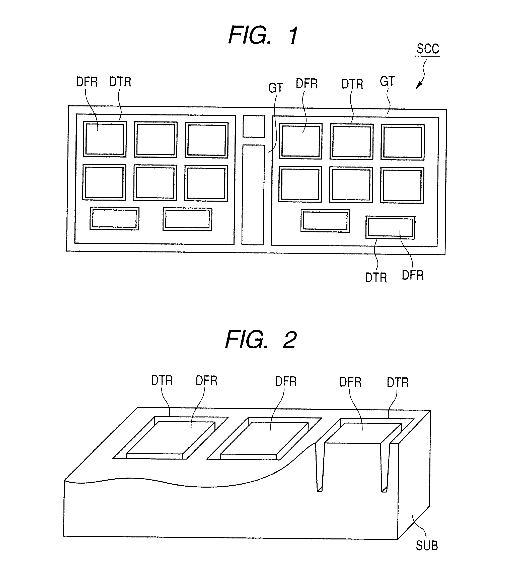
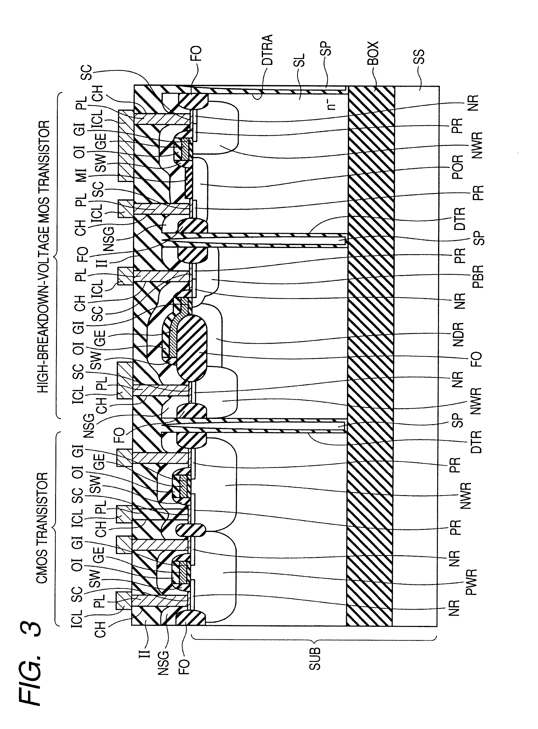
[0095]As illustrated in FIG. 1, the semiconductor device of the present embodiment can be applied to, for example, BiC-DMOS (bipolar complementary double-diffused metal oxide semiconductor). A semiconductor chip SCC of this BiC-DMOS has, for example, a logic portion in which low-breakdown-voltage CMOS (complementary MOS) transistors have been integrated and an output driver portion using a high breakdown voltage element. In the output driver portion, element formation regions DFR which are formation regions for individual elements are each surrounded by a trench DTR having a DTI structure in planar view. In addition, a plurality of the element formation regions DFR is surrounded by a gettering site in a planar view.

[0096]As illustrated in FIG. 2, for example, in the output driver portion, the element formation regions DFR for individual high-breakdown-voltage elements are surrounded two-dimensionally by the trench DTR having a DTI structure. This trench DTR is formed in the surface ...

embodiment 2

[0158]The present embodiment is different from Embodiment 1 in the configuration and production method of the trench DTR and the underlying oxide film NSG. The configuration of the present embodiment will next be described.

[0159]In Embodiment 1, as illustrated in FIG. 24, a width W1 of the trench DTR in the semiconductor layer SL is almost equal to a width W2 of the underlying oxide film NSG. On the other hand, in the trench DTR of Embodiment 2, the width W1 of the bottom portion (the lowermost part) of the trench DTR is greater than the width W2 (width of an opening penetrating through the underlying oxide film NSG) of the trench DTR in the underlying oxide film NSG (second insulating film) as can be seen from FIGS. 25 and 26.

[0160]Supposing that the width W2 of the opening (the trench DTR in the underlying oxide film NSG) of the underlying oxide film NSG as illustrated in FIGS. 25 and 26 is as large as the width W2 of the opening of the underlying oxide film NSG of FIG. 24 in Embo...

embodiment 3

[0188]The present embodiment differs from Embodiment 1 in the configuration and manufacturing method of the trench DTR and underlying oxide film NSG. The configuration of this embodiment will next be described.

[0189]As illustrated in FIGS. 55 and 56, in the trench DTR of Embodiment 3, the width (the width of an opening penetrating through the underlying oxide film NSG) of the trench DTR in the underlying oxide film NSG (second insulating film) is greater than the width (width, at the upper most portion closest to the underlying oxide film NSG, of the trench DTR formed in the semiconductor layer SL) at the opening ends of the trench DTR. In this point, the trench DTR of Embodiment 3 is different from the trench DTR of Embodiment 1 illustrated in FIG. 24 or the trench DTR of Embodiment 2 illustrated in FIG. 25.

[0190]The width (width, at the upper most portion closest to the underlying oxide film NSG, of the trench DTR formed in the semiconductor layer SL) at the opening ends of the tr...


PUM


Abstract

To provide a semiconductor device that can be manufactured using a simple process without ensuring a high embedding property; and a manufacturing method of the device. In the manufacturing method of the semiconductor device according to the invention, a semiconductor substrate having a configuration obtained by stacking a support substrate, a buried insulating film, and a semiconductor layer in order of mention is prepared first. Then, an element having a conductive portion is completed over the main surface of the semiconductor layer. A trench encompassing the element in a planar view and reaching the buried insulating film from the main surface of the semiconductor layer is formed. A first insulating film (interlayer insulating film) is formed over the element and in the trench to cover the element and form an air gap in the trench, respectively. Then, a contact hole reaching the conductive portion of the element is formed in the first insulating film.

Description

CROSS-REFERENCE TO RELATED APPLICATIONS[0001]The disclosure of Japanese Patent Application No. 2010-10085 filed on Jan. 20, 2010 including the specification, drawings and abstract is incorporated herein by reference in its entirety.BACKGROUND OF THE INVENTION[0002]The present invention relates to a semiconductor device and a manufacturing method thereof, in particular, to a semiconductor device having a trench and a manufacturing method of the device.[0003]For example, Japanese Patent Laid-Open No. 2002-118256 discloses an element isolation (deep trench isolation: DTI) structure obtained by filling an insulating film in a trench with a high aspect ratio.[0004]According to the technology described in the document, first, a trench is formed in the surface of a semiconductor substrate. A first insulating film is then formed over the surface of the semiconductor substrate so as to embed the trench with the film. The first insulating film is then anisotropically etched to form, in the fi...

Claims


Application Information

Patent Timeline
IPC IPC(8): H01L29/06H01L21/76
CPCH01L21/76232H01L21/76283H01L21/823878H01L22/34H01L2924/0002H01L27/1203H01L2924/00
Inventor MORII, KATSUMIOTSU, YOSHITAKAONISHI, KAZUMANITTA, TETSUYASHIROMOTO, TATSUYATOKUMITSU, SHIGEO
Owner RENESAS ELECTRONICS CORP
Why Eureka
Try Eureka