Interface circuit, lsi, server device, and method of training the interface circuit

a technology of interface circuit and server device, which is applied in the direction of digital transmission, pulse automatic control, instruments, etc., can solve the problems of unnecessarily large increase power consumption of interface circuit and/or a whole of server device, and increase power consumption of interface circuit and/or server device. , to achieve the effect of increasing the size of the waveform shaping circuit and increasing the power consumption

Inactive Publication Date: 2011-07-28
HITACHI LTD
View PDF4 Cites 0 Cited by
  • Summary
  • Abstract
  • Description
  • Claims
  • Application Information

AI Technical Summary

Benefits of technology

[0004]When aiming to achieve the signal processing technology as described above, a problem has been raised that power consumption is increased due to influence of a circuit (waveform shaping circuit, hereinafter) added for waveform adjustment and / or waveform shaping. In the server device, while a plurality of boards are connected to the backplane and thus short and long transfer distances are mixed among boards, it is not that the boards can be exchanged in accordance with distances but that a common board is used. Therefore, an interface circuit provided to each board for transferring signals among boards is necessary to be prepared in a configuration capable of meeting the longest transfer distance. The longer a transfer distance between boards, the larger the size of a waveform shaping circuit. Therefore, waveform shaping circuits having a size meeting the longest transfer distance between boards are prepared in the interface circuit, and they will be used in a place where a transfer distance is short. In this manner, there are problems raised that power consumption is wasted by a waveform shaping circuit having an unnecessarily large size, and, power consumption of an LSI having the interface circuit and / or a whole of the server device is increased.

Problems solved by technology

When aiming to achieve the signal processing technology as described above, a problem has been raised that power consumption is increased due to influence of a circuit (waveform shaping circuit, hereinafter) added for waveform adjustment and / or waveform shaping.
In this manner, there are problems raised that power consumption is wasted by a waveform shaping circuit having an unnecessarily large size, and, power consumption of an LSI having the interface circuit and / or a whole of the server device is increased.

Method used


Image

  • Interface circuit, lsi, server device, and method of training the interface circuit
  • Interface circuit, lsi, server device, and method of training the interface circuit
  • Interface circuit, lsi, server device, and method of training the interface circuit

Examples


Embodiment Construction

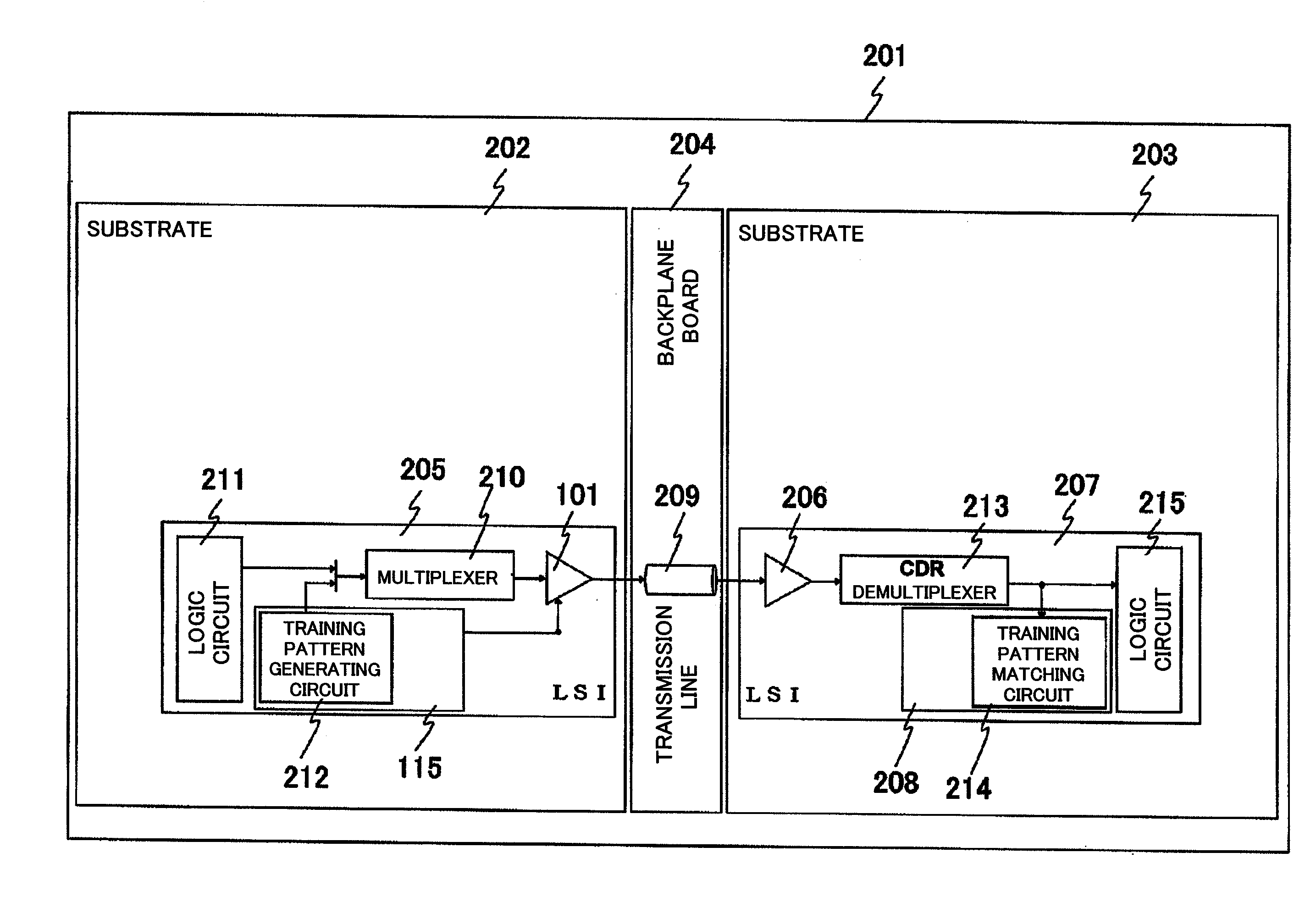
[0010]FIG. 1 illustrates an embodiment of an interface output circuit 101 of the present invention. The interface output circuit 101 includes three CML (current mode logic) circuits. They are a CML circuit 102 of a signal output circuit which outputs signals as voltage amplitude, a CML circuit 103 connected to the CML circuit 102 and used in a waveform shaping circuit, and a CML circuit 104. The interface output circuit 101 includes a flip-flop circuit 105 which retains, i.e., latches a data input signal to the interface output circuit 101, a flip-flop circuit 106, and a flip-flop circuit 107. The data input signal is first inputted to the flip-flop circuit 105.

[0011]In the present embodiment, the three flip-flop circuits 105, 106, and 107 are connected in series, and in a configuration of a shift circuit in which the data input signal reaches an output of the flip-flop circuit 107 by three clock signals. An output signal of the flip-flop circuit 105 retains a signal prior to the cu...


PUM


Abstract

Power consumption is increased in an interface circuit having a signal processing function for waveform shaping due to influence of a circuit added for waveform shaping. Also, since a plurality of boards are connected to a backplane in a system, they are not exchanged in accordance with distances while there are boards being far or near are mixed, but a common board is used. Thus, it is necessary to prepare a configuration of an interface circuit meeting the longest transfer distance. An interface circuit disabling a part of or all of operations of a waveform shaping circuit is provided. Accordingly, in accordance with transfer distances, switching of operation ranges of waveform shaping circuit inside the interface circuit is possible, and operation ranges of the waveform shaping circuit can be limited, and power consumption of the interface circuit, an LSI including the interface circuit, and a server device can be reduced.

Description

CROSS-REFERENCE TO RELATED APPLICATION[0001]The present application claims priority from Japanese Patent Application No. 2010-014991 filed on Jan. 27, 2010, the content of which is hereby incorporated by reference into this application.TECHNICAL FIELD OF THE INVENTION[0002]The present invention relates to an interface circuit, an LSI including the interface circuit, a server device, and a method of training the interface circuit.BACKGROUND OF THE INVENTION[0003]In recent years, larger capacities of data and faster speed of communications in computer network communications have been desired. Here, in data processing on a network, performance of inter-device communication of server devices supporting data communications has been a bottle neck. In the server device, a plurality of boards are connected to a printed circuit board, called backplane, to which a connector and a slot provided in a chassis of the server device are attached. In data communication in the server device, transfer...

Claims


Application Information

Patent Timeline
Patent Type & Authority Applications(United States)
IPC IPC(8): H03L5/00
CPCH04L25/0288H04L25/03343H04L25/03038
Inventor WATANABE, KEIKIMUTO, TAKASHIKOBA, HIDEKI
Owner HITACHI LTD
Why Eureka
Try Eureka