Semiconductor device and driving method thereof, electro-optical device, and electronic device

a technology of electromagnetic field and driving method, applied in the direction of oscillator, pulse technique, instruments, etc., can solve the problems of insufficient data voltage to be applied to a liquid crystal element which is a capacitive element, and inability to reduce parasitic capacitance variations

Inactive Publication Date: 2011-07-28
SEIKO EPSON CORP
View PDF3 Cites 4 Cited by
  • Summary
  • Abstract
  • Description
  • Claims
  • Application Information

AI Technical Summary

Benefits of technology

[0009]An advantage of some aspects of the invention is that it provides a semiconductor device capable of applying a data voltage to a capacitive element via a TFT more reliably and a driving method thereof, an electro-optical device and an electronic device having the semiconductor device.

Problems solved by technology

In such liquid crystal apparatus, due to a parasitic capacitance between a gate and a drain of a TFT as a pixel switching element or between the gate and a source thereof, a feed-through voltage is generated, and there is a technical problem in that a data voltage to be applied to a liquid crystal element which is a capacitive element may be insufficient.
However, in the technique disclosed in Japanese Patent No. 3656179, there are problems in that it is difficult to reduce variations in parasitic capacitance caused by variations in production of TFTs, and variations in feed-through voltage may remain.
Accordingly, there is a concern that a data voltage may be insufficiently applied to a liquid crystal element which is a capacitive element.

Method used


Image

  • Semiconductor device and driving method thereof, electro-optical device, and electronic device
  • Semiconductor device and driving method thereof, electro-optical device, and electronic device
  • Semiconductor device and driving method thereof, electro-optical device, and electronic device

Examples


first embodiment

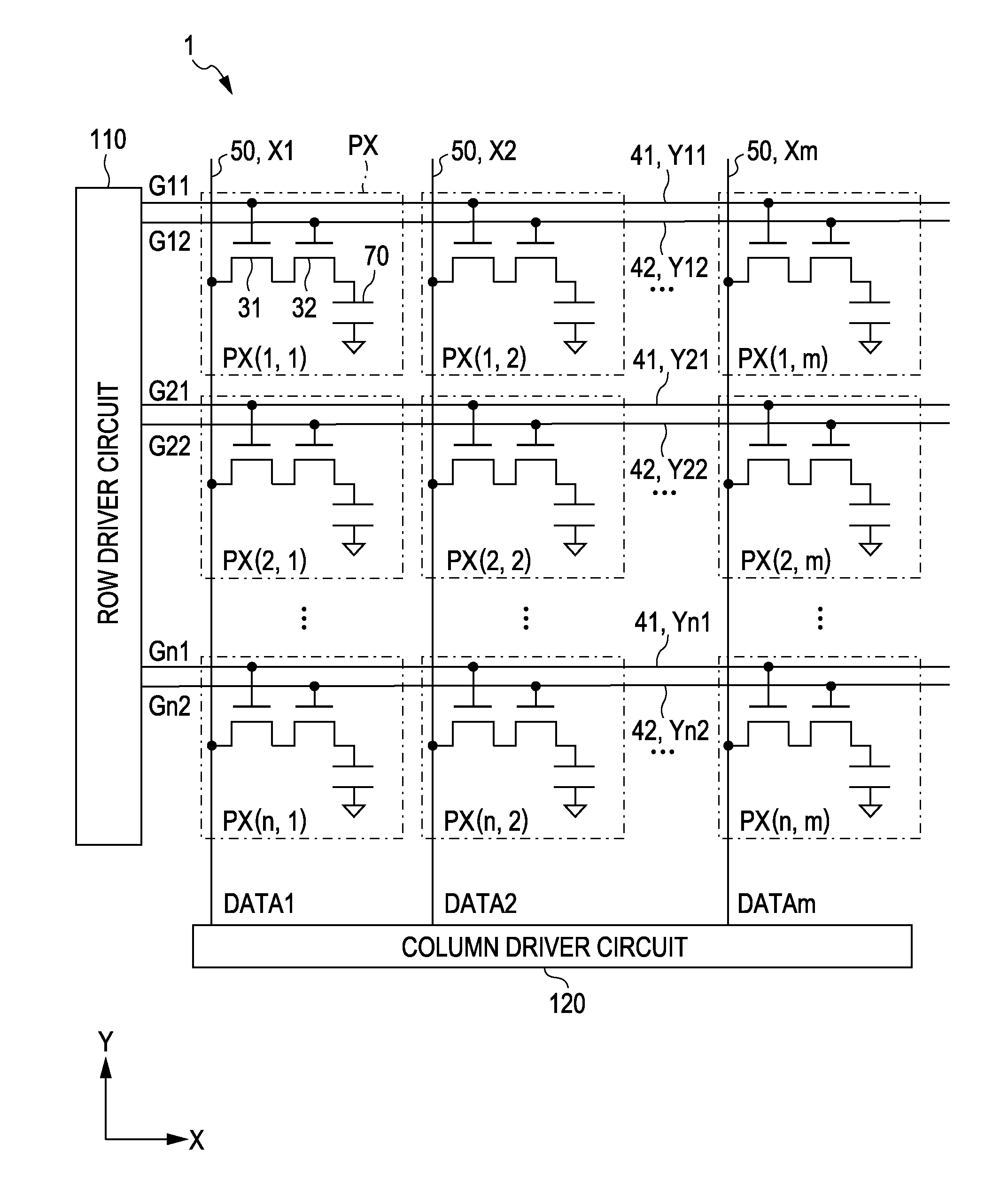
[0051]A semiconductor device according to a first embodiment will be described with reference to FIGS. 1 to 8.

[0052]First, the entire configuration of the semiconductor device according to this embodiment is described with reference to FIG. 1.

[0053]FIG. 1 is a diagram illustrating the configuration of the semiconductor device according to this embodiment.

[0054]In FIG. 1, the semiconductor device 1 according to this embodiment includes a plurality of unit circuits PX (that is, PX(1,1), PX(1,2), . . . , PX(n,m-1), PX(n,m)) arranged in a matrix (two-dimensional plane) with n rows and m columns (here, m and n are natural numbers), n first gate lines 41 (that is, first gate lines Y11, Y21, . . . , Yn1), n second gate lines 42 (that is, second gate lines Y12, Y22, . . . , Yn2), m data lines 50 (that is, data lines X1, X2, . . . , Xm), a row driver circuit 110, and a column driver circuit 120. The first gate lines 41, the second gate lines 42, the row driver circuit 110, and the column dri...

first modified example

[0089]FIG. 9 is a diagram illustrating a unit circuit of a semiconductor device according to a first modified example.

[0090]As illustrated in FIG. 9, the unit circuit PX may include a storage capacitor 71 and a liquid crystal element 72 instead of the capacitive element 70 in the first embodiment described above with reference to FIG. 1. In this case, a liquid crystal display apparatus can be realized using the semiconductor device. Here, according to this modified example, even if parasitic capacitances of the first and second transistors 31 and 32 vary due to the variations in production, the data voltage can be reliably applied to the storage capacitor 71 which is a capacitive element and the liquid crystal element 72 via the first and second transistors 31 and 32 from the data line 50, so that non-uniform display such as so-called “screen burn-in” can be reduced or prevented.

second modified example

[0091]FIG. 10 is a diagram illustrating a unit circuit of a semiconductor device according to a second modified example.

[0092]As illustrated in FIG. 10, the unit circuit PX may include a storage capacitor 71 and an electrophoretic element 74 instead of the capacitive element 70 in the first embodiment described above with reference to FIG. 1. In this case, an electrophoretic display apparatus can be realized using the semiconductor device. Here, according to this modified example, even if parasitic capacitances of the first and second transistors 31 and 32 vary due to the variations in production, the data voltage can be reliably applied to the storage capacitor 71 which is a capacitive element and the electrophoretic element 74 via the first and second transistors 31 and 32 from the data line 50, so that non-uniform display can be reduced or prevented.


PUM


Abstract

A semiconductor device includes: a first transistor which is electrically connected between a capacitive element and a data line; a second transistor which is electrically connected between the first transistor and the capacitive element; and a driving unit. The driving unit drives the first and second transistors so that when the data voltage is applied to the capacitive element, both the first and second transistors are turned on, the second transistor is temporarily turned off, after a timing at which both the first and second transistors are turned on, and then turned on again, and the first transistor is turned off at the timing at which the second transistor is temporarily turned off or after the timing and before the second transistor is turned on again.

Description

CROSS-REFERENCE TO RELATED APPLICATION[0001]This application is based on and claims priority from Japanese Patent Application No. 2010-014360, filed on Jan. 26, 2010, the contents of which are incorporated herein by reference.BACKGROUND[0002]1. Technical Field[0003]The present invention relates to the technical field of a semiconductor device and a driving method thereof, an electro-optical device, and an electronic device.[0004]2. Related Art[0005]A liquid crystal apparatus in an active matrix drive type is an example of a semiconductor device. In the liquid crystal apparatus, a pixel electrode is provided for each pixel on a substrate, and scanning lines, data lines, and thin film transistors (TFT) as pixel switching elements are included for selectively driving the pixel electrodes, thereby realizing active matrix driving.[0006]In such liquid crystal apparatus, due to a parasitic capacitance between a gate and a drain of a TFT as a pixel switching element or between the gate and ...

Claims


Application Information

Patent Timeline
IPC IPC(8): G09G5/00H03K17/687
CPCG09G3/3648G09G2310/0262G09G2320/0233G09G2320/0219G09G2320/0209
InventorOZAWA, TOKUROSATO, TAKASHI
OwnerSEIKO EPSON CORP